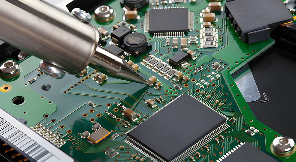
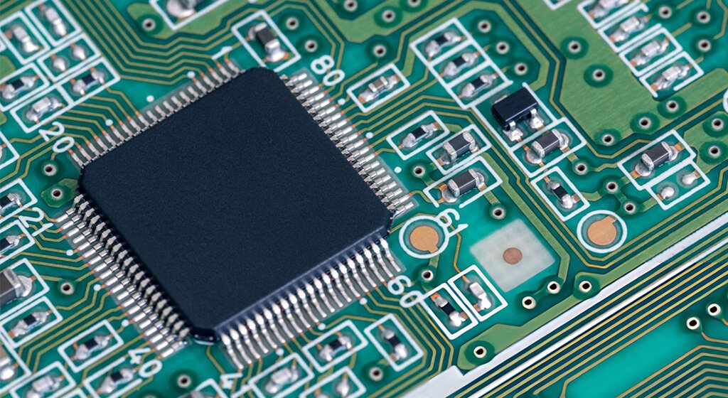
A surface mount device (SMD) is an electronic component soldered directly onto pads on a printed circuit board.
A phone or medical monitor may carry thousands of these parts inside a surprisingly small board area.
That density brings practical trade-offs involving package selection, paste control, moisture handling, heat, and inspection.
Table of Contents
1. What Does SMD Mean in Electronics?
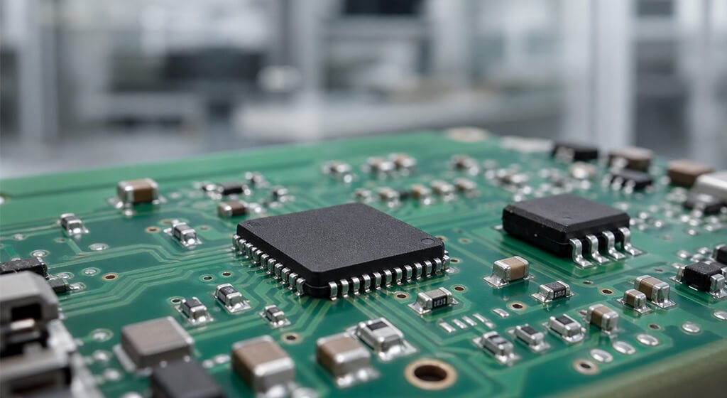
SMD stands for surface mount device, meaning a component whose terminals connect directly with pads on a PCB surface.
The component may have short leads, flat terminations, solder balls, or metal contacts underneath its molded body.
SMDs includes passive parts, semiconductors, electromechanical devices, sensors, LEDs, connectors, and many specialized electronic components.
Our SMT components guide examines component selection, package families, sourcing risks, and practical assembly considerations.
2. SMD vs SMT: What Is the Difference?
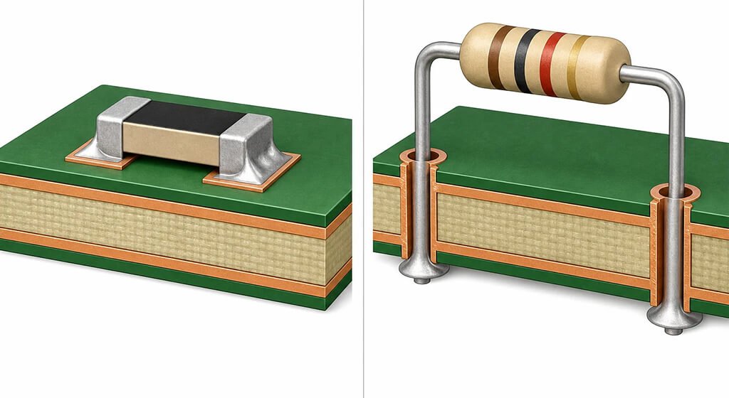
SMD and SMT are closely related terms, but they describe different parts of the electronics manufacturing process.
An SMD is the physical component, while SMT describes the technology used to mount that component onto a PCB.
Term | Full Name | Meaning |
SMD | Surface Mount Device | A component designed for mounting directly onto PCB pads |
SMT | Surface Mount Technology | The process used to place and solder SMDs onto a PCB |
SMC | Surface Mount Component | Another common term describing a component intended for surface mounting |
SMA | Surface Mount Assembly | A completed board or module assembled using surface mount technology |
THT | Through-Hole Technology | A process inserting component leads through drilled PCB holes |
A chip resistor is an SMD, while solder paste printing and reflow are stages within the SMT process.
Keeping these terms separate prevents ambiguity across bills of materials, assembly drawings, inspection requirements, and supplier instructions.
Do You Need Any Help?
3. How Does a Surface Mount Device Connect to a PCB?
Every SMD needs electrical terminals that align with a corresponding land pattern on the printed circuit board.
Those terminals may appear along two edges, four edges, underneath the package, or across an array of solder balls.
During assembly, solder paste provides solder alloy and flux between each component termination and its matching copper pad.
A placement machine positions the component, and controlled reflow heating creates permanent electrical and mechanical solder joints.
Surface tension can correct small placement offsets, provided the pad geometry and solder volumes remain reasonably balanced.
The finished joints carry current, transfer signals, conduct heat, and often provide the component’s primary mechanical support.
4. Main Types of Surface Mount Devices
Surface mount devices can be grouped by electrical function, although their packages may look surprisingly similar externally.
4.1. Passive SMD Components
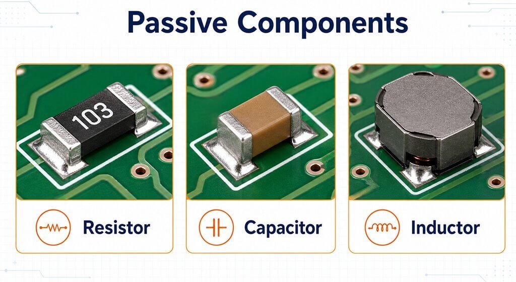
Passive components manage current, voltage, filtering, timing, energy storage, and unwanted electrical noise without providing amplification.
Common passive SMDs include resistors, capacitors, inductors, ferrite beads, thermistors, fuses, and frequency-control components used throughout modern circuits.
Chip resistors usually have rectangular ceramic bodies with metal terminations covering both short ends of each device.
Multilayer ceramic capacitors look similar, but their unmarked bodies make visual value identification difficult or impossible.
Inductors and ferrite beads support power conversion, filtering, and electromagnetic interference control across many modern circuits.
4.2. Active SMD Components
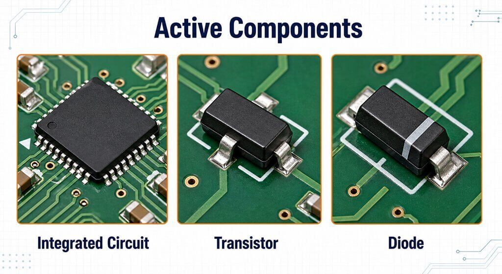
Active devices control, switch, amplify, regulate, sense, store, or process signals within an electronic system, such as diodes, transistors, MOSFETs, voltage regulators, microcontrollers, processors, memories, sensors, and communication integrated circuits.
Package choices range from SOT, SOIC, and TSSOP through QFP, QFN, BGA, LGA, and chip-scale formats.
Package choice affects routing density, thermal resistance, assembly difficulty, inspection access, and long-term field performance.
4.3. Electromechanical and Optoelectronic SMDs
Surface mount production also supports switches, connectors, relays, microphones, antennas, crystals, LEDs, and optocouplers used in modern products.
Such devices may face mechanical loads, optical alignment requirements, polarity constraints, or special handling during production.
Larger connectors sometimes require additional anchors because their solder joints should not carry repeated mating forces alone.
5. Common SMD Package Sizes
Two-terminal chip components commonly use four-digit case codes representing nominal length and width in hundredths of inches.
Metric codes use tenths of millimeters, creating frequent confusion between imperial and metric naming conventions.
The table combines official Vishay 01005 and Vishay 0201–1206 resistor dimensions used throughout the electronics industry.
Imperial Case Code | Metric Code | Approximate Body Size | General Manufacturing Characteristic |
01005 | 0402M | 0.4 × 0.2 mm | Extremely small and demanding to place, inspect, and rework |
0201 | 0603M | 0.6 × 0.3 mm | Common in highly compact, high-density electronic products |
0402 | 1005M | 1.0 × 0.5 mm | Small footprint requiring precise solder paste control |
0603 | 1608M | Approximately 1.6 × 0.8 mm | Popular balance between component density and manufacturability |
0805 | 2012M | Approximately 2.0 × 1.25 mm | Easier to inspect, handle, solder, and rework |
1206 | 3216M | Approximately 3.2 × 1.6 mm | Larger area supporting broader electrical and thermal options |
A package code identifies a size family, while actual dimensions and tolerances remain specific to each product series.
Designers should never build a production footprint from the four-digit case code without reviewing the component datasheet.
Do You Need Any Help?
6. Why Does Package Size Not Determine Power Rating?
Size usually tracks power capacity, but two equally sized resistors can carry very different ratings.
Vishay lists different P70 ratings for identical case sizes across its precision and high-stability resistor families.
Case Size | Precision Series P70 | High-Stability AT Series P70 |
0402 | 0.063 W | 0.130 W |
0603 | 0.100 W | 0.210 W |
0805 | 0.125 W | 0.260 W |
1206 | 0.250 W | 0.520 W |
These figures come from Vishay’s precision thin-film series and high-stability AT series datasheets, not a generic package chart.
Check resistance, voltage, pulse capability, derating, ambient temperature, and PCB thermal design before approving any substitute.
7. What Surface Mount Package Types Are Common?
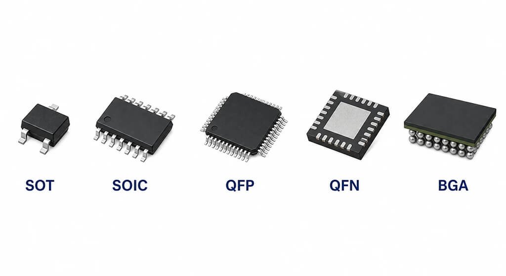
Integrated circuits use several terminal arrangements, each creating different layout, inspection, thermal, and rework requirements.
Package Family | Terminal Arrangement | Main Advantage | Main Assembly Consideration |
SOT | Leads extending from two sides | Compact package for transistors and small ICs | Polarity and orientation require verification |
SOIC | Gull-wing leads on two sides | Visible joints and familiar assembly process | Body width and pitch vary between series |
TSSOP | Fine gull-wing leads on two sides | Higher density than conventional SOIC packages | Fine pitch increases bridging sensitivity |
QFP | Gull-wing leads around four sides | High pin count with visually accessible leads | Coplanarity and handling affect placement quality |
QFN or DFN | Flat terminals underneath package edges | Small footprint with strong thermal options | Hidden joints need controlled paste and inspection |
BGA | Solder balls arranged underneath the package | High connection density and efficient routing | X-ray inspection is commonly required |
LGA | Flat lands arranged underneath the package | Low package height without attached solder balls | Paste volume and pad finish require tight control |
CSP or WLCSP | Package dimensions approach die dimensions | Extremely compact size and short interconnections | Board finish, warpage, handling, and underfill may matter |
Texas Instruments maintains an official packaging terminology reference covering common package family names for engineers evaluating component options.
For BGA designs, IPC-7095E addresses implementation, inspection, rework, and reliability considerations associated with hidden solder connections.
8. How Does the Surface Mount Technology Process Work?
SMT production moves bare boards and packaged components through five controlled stages ending with inspection and electrical testing.
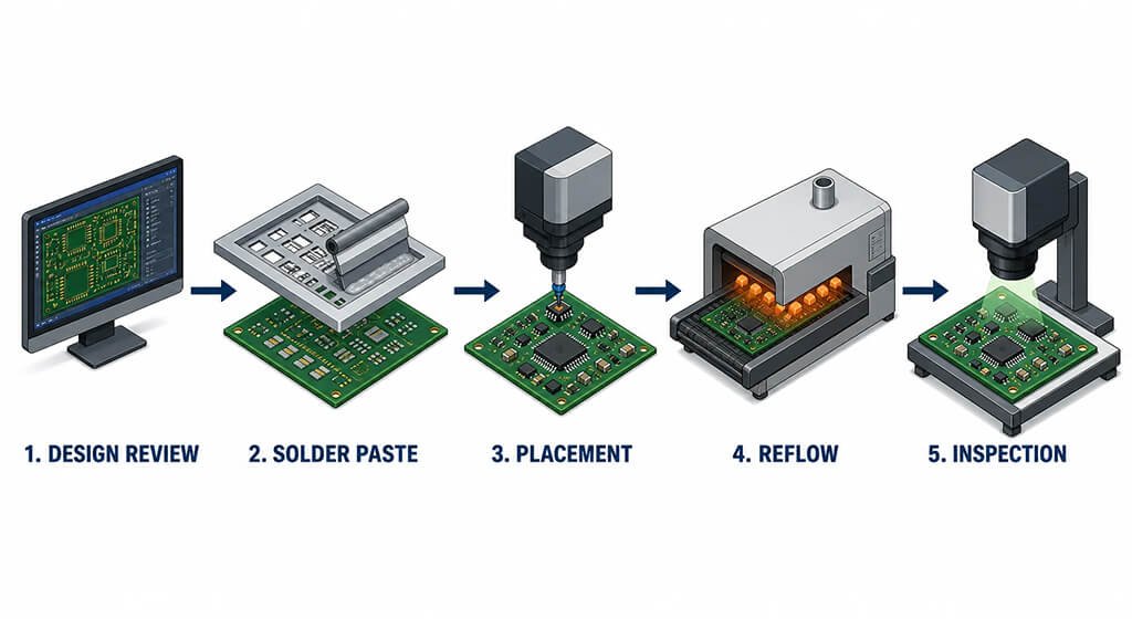
Step 1. Design and Production Data Review
Engineers review Gerber data, the bill of materials, centroid coordinates, polarity information, panelization, and assembly drawings.
This review exposes footprint conflicts, unavailable parts, rotation errors, thermal risks, and inspection gaps before production.
Step 2. Solder Paste Printing
A stencil printer deposits measured solder paste volumes onto copper pads at each planned component location.
Stencil thickness, aperture geometry, paste type, board support, and printing parameters strongly influence subsequent solder joint quality.
Three-dimensional solder paste inspection can measure deposit height, area, volume, alignment, and suspicious bridging before placement.
Step 3. Automated Component Placement
Pick-and-place machines pull components from reels, trays, or tubes before setting them onto printed solder paste.
Vision systems identify component centers, terminal features, orientation marks, and board fiducials during high-speed automated placement.
Published equipment specifications show automation’s scale, although actual throughput depends heavily on each product configuration.
Yamaha rates its YRM20DL at 120,000 components hourly and ±0.015-millimeter placement accuracy under published specifications.
Real output changes with feeder setup, board geometry, component mix, inspection requirements, and production changeovers.
Step 4. Reflow and Surface Mount Device Soldering
The loaded board travels through controlled heating zones, where flux activates and molten solder forms permanent connections.
Each profile must consider solder paste chemistry, PCB thermal mass, component ratings, board finishes, and temperature uniformity.
IPC/JEDEC classification profiles define component limits, but they are not universal production recipes for every assembly.
Texas Instruments reports approximately 217°C as a common lead-free liquidus temperature within its reflow guidance.
TI also limits ramp-up to 3°C per second and permits eight minutes maximum from room temperature through peak.
The final oven recipe must match component limits and the solder paste supplier’s recommended processing window.
Step 5. Inspection and Electrical Testing
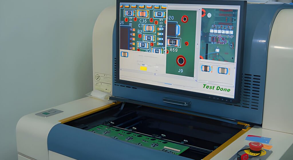
Automated optical inspection detects missing parts, polarity errors, misalignment, lifted leads, bridging, and visible solder anomalies.
X-ray inspection evaluates hidden joints beneath BGA, LGA, QFN, and other bottom-terminated surface mount devices.
In-circuit testing, flying-probe testing, functional testing, or customized fixtures can verify electrical performance after visual inspection.
PCBSAIL’s SMT assembly service explains its DFM, SPI, placement, reflow, AOI, X-ray, and testing workflow.
Do You Need Any Help?
9. What Are the Main Advantages of Surface Mount Devices?
Designers choose SMDs when products demand miniaturization, scalable automation, dense electronic layouts, and repeatable manufacturing.
9.1. Smaller Products and Higher Density
Compact packages occupy less board area and allow components on both sides of a printed circuit board.
Removing most drilled component holes also preserves routing space for signal, power, and ground connections between board layers.
9.2. Efficient Automated Production
Standardized tape, tray, and tube packaging allows machines to feed and place thousands of different component types.
Good data, stable feeders, controlled processes, and effective inspection let automation deliver repeatable production at useful speeds.
9.3. Improved High-Frequency Performance
Shorter interconnections can reduce parasitic inductance and unwanted loop area compared with long through-hole component leads.
Signal integrity still depends on package geometry, PCB stack-up, return paths, via placement, and routing.
9.4. Lower Cost at Suitable Volumes
Automated placement can reduce repetitive manual labor and support economical production across medium and high manufacturing volumes.
Small prototype runs still carry setup, programming, stencil, inspection, and engineering costs across relatively few boards.
10. What Limitations Do Surface Mount Devices Have?
10.1. More Difficult Manual Rework
Small bodies and narrow pitches require magnification, temperature control, suitable tooling, skilled operators, and documented rework procedures.
Nearby components can move or overheat when manual rework introduces excessive airflow, contact, or uncontrolled thermal exposure.
10.2. Mechanical Loading Concerns
Surface-mount solder joints often carry both current and mechanical loads, so connector stress deserves early attention.
Connectors, transformers, switches, and heavy components may require through-hole anchors, brackets, adhesives, or other mechanical reinforcement.
10.3. Hidden Solder Joints
QFN, LGA, CSP, and BGA packages place important connections underneath their bodies, limiting direct optical inspection.
They need appropriate stencil design, reflow control, X-ray strategy, and sometimes specialized electrical or functional testing.
10.4. Moisture Sensitivity
Some nonhermetic semiconductor packages absorb moisture after leaving their sealed moisture-barrier bags and controlled storage environments.
Rapid heating can damage an overexposed package, making floor-life tracking and approved baking procedures operationally important.
11. How Do Moisture Sensitivity Levels Affect SMD Components?
Texas Instruments reproduces widely used floor-life values from IPC/JEDEC J-STD-033 within its official moisture handling guidance.
MSL | Maximum Floor Life After Opening | Specified Environment |
1 | Unlimited | No more than 30°C and 85% RH |
2 | One year | No more than 30°C and 60% RH |
2A | Four weeks | No more than 30°C and 60% RH |
3 | 168 hours | No more than 30°C and 60% RH |
4 | 72 hours | No more than 30°C and 60% RH |
5 | 48 hours | No more than 30°C and 60% RH |
5A | 24 hours | No more than 30°C and 60% RH |
6 | Bake before use, then reflow within the labeled time | Follow the component label |
TI’s MSL application report gives MSL 3 components a 168-hour floor life under those stated conditions.
Exceeding that allowance may require controlled baking, but the package label and current manufacturer instructions remain authoritative.
12. SMD vs Through-Hole: Which Mounting Method Fits Your Design?
The right mounting method depends on electrical needs, mechanical loads, production volumes, serviceability, and the operating environment.
Design Factor | Surface Mount Device | Through-Hole Component |
Mounting method | Soldered directly onto surface pads | Leads pass through drilled and plated holes |
Typical size | Generally smaller and lighter | Generally larger with longer leads |
Component density | High, including double-sided placement | Lower because holes consume routing area |
Automated placement | Highly compatible | Possible, but often less flexible |
Manual prototyping | More difficult for small packages | Usually easier to handle and replace |
Mechanical anchoring | Primarily supported by soldered lands | Leads provide stronger board anchoring |
Hidden joints | Common with QFN, LGA, and BGA | Most joints remain accessible underneath |
Typical preference | Compact, high-density, scalable products | Heavy, high-power, or mechanically stressed parts |
Many assemblies combine both technologies, using SMDs for density and through-hole parts for demanding mechanical connections.
Our detailed SMT versus through-hole comparison explains selection factors, applications, and hybrid assembly in greater technical detail.
PCBSAIL also offers dedicated through-hole PCB assembly for mechanically demanding parts within mixed-technology product designs.
Do You Need Any Help?
13. Which Design Rules Improve Reliable SMD Assembly?
A good component cannot rescue an incorrect footprint, incomplete production package, or poorly planned thermal path.
13.1. Use the Exact Manufacturer Footprint
IPC-7352 provides general land-pattern principles covering component attachment and dependable solder joint formation across modern assemblies.
IPC recommends checking manufacturer datasheets because production packages sometimes differ from their standardized component outlines.
Verify body dimensions, lead geometry, pin pitch, exposed pads, tolerances, courtyard, and recommended stencil information.
13.2. Provide Clear Orientation Information
Keep pin-one symbols, polarity marks, centroid rotations, assembly drawings, and silkscreen references consistent across every file.
Conflicting orientation data slows first-article approval and raises placement risk before the production line even starts.
13.3. Plan Thermal Paths Early
Power devices may need exposed pads, thermal vias, heavier copper, internal spreading planes, airflow, or external heat sinks.
Thermal-pad paste coverage should balance heat transfer, solder voiding, component float, and manufacturable stencil aperture designs.
13.4. Match Inspection to Package Geometry
Visible gull-wing leads suit optical inspection, while bottom-terminated components often require X-ray and additional process monitoring.
Choose inspection during design because finished package geometry may permanently hide critical solder joints from cameras.
13.5. Control the Approved Bill of Materials
Substitutes must match electrical ratings, package dimensions, polarity, moisture sensitivity, temperature limits, and assembly compatibility requirements.
Your procurement package needs manufacturers, exact part numbers, approved alternatives, traceability rules, and date-code restrictions.
PCBSAIL’s turnkey PCBA service coordinates component sourcing, board fabrication, assembly, inspection, and testing within one managed workflow.
14. What Are the Most Common SMD Assembly Defects?
Most defects result from interactions among PCB design, materials, printing, placement, reflow, handling, and inspection effectiveness.
Defect | Typical Contributing Factors | Common Detection Method |
Solder bridging | Excess paste, narrow spacing, poor alignment, or unsuitable apertures | AOI and electrical testing |
Tombstoning | Unequal wetting forces, pad imbalance, or uneven heating | AOI or visual inspection |
Insufficient solder | Poor paste transfer, blocked aperture, or inadequate stencil design | SPI and AOI |
Misaligned component | Placement offset, weak fiducials, movement, or unstable printing | Pre-reflow and post-reflow AOI |
Open joint | Contamination, coplanarity problems, insufficient paste, or poor wetting | AOI, X-ray, ICT, or functional testing |
Voiding | Volatile entrapment, pad geometry, paste selection, or thermal profile | X-ray inspection |
Wrong polarity | Inconsistent files, unclear markings, or feeder setup errors | AOI, first-article inspection, and testing |
SPI catches printing problems, AOI sees visible faults, and X-ray reveals joints hidden underneath packages.
15. Which Standards Apply to Surface Mount Devices?
These standards cover land patterns, soldering, inspection, moisture handling, and specialized package implementation across production lines.
Standard | Main Relevance |
IPC-7352 | Generic guidelines for surface-mount and through-hole land-pattern design |
IPC J-STD-001J | Requirements for soldered electrical and electronic assemblies |
IPC-A-610J | Post-assembly acceptability criteria for electronic assemblies |
IPC-7525C | Stencil design guidance for solder-paste application |
IPC-7530B | Temperature-profiling guidance for mass-soldering processes |
IPC-7095E | Design and assembly guidance for BGA and fine-pitch BGA packages |
IPC/JEDEC J-STD-020F | Moisture and reflow sensitivity classification for plastic SMD packages |
IPC/JEDEC J-STD-033D | Packaging and handling guidance for moisture-sensitive surface-mount devices |
IPC’s official document revision table lists current and historical revisions for standards used throughout electronics manufacturing.
IPC identifies J-STD-001J for soldering requirements and IPC-A-610J for post-assembly acceptance criteria across electronic assemblies.
IPC’s 2024 revision announcement recommends using both documents together during manufacturing and post-assembly inspection programs.
16. How Do Lead-Free Rules Affect SMD Assemblies?
Many modern SMD assemblies use lead-free terminations and solder alloys to meet environmental and customer compliance requirements.
The European RoHS Directive limits lead to 0.1 percent within homogeneous materials, subject to specified exemptions.
Cadmium is limited to 0.01 percent, while several other restricted substances carry 0.1-percent thresholds.
The official limits, exemptions, and subsequent amendments appear within the published European Union RoHS Directive.
Compliance declarations should reference the exact part, material, supplier documentation, applicable exemption, and current regulatory revision.
17. Where Are Surface Mount Devices Used?
Consumer products use them in phones, wearables, computers, cameras, appliances, entertainment systems, and smart home devices.
Automotive and medical systems use them within control units, sensors, monitors, portable diagnostics, imaging, and communication hardware.
Industrial and telecommunications products rely on SMDs for controllers, robotics, power supplies, radios, routers, and optical equipment.
Some power designs combine SMD control electronics with through-hole connectors, transformers, capacitors, or mechanically stressed components.
19. How Should You Choose an SMD Assembly Partner?
Placement speed alone says little about whether a supplier can repeatedly build and inspect your difficult board.
Review each supplier’s DFM process, material controls, paste inspection, thermal profiling, AOI, X-ray capability, and electrical testing.
Also examine traceability, substitute approval, moisture tracking, ESD protection, engineering changes, first articles, and documented rework.
PCBSAIL handles prototypes and production through SMT assembly services covering sourcing, placement, inspection, and testing.
Clean Gerber files, a controlled BOM, centroid data, assembly drawings, and test requirements make engineering review faster.
20. FAQ About Surface Mount Devices?
Is an SMD the same as SMT?
No, an SMD is the component, while SMT is the manufacturing technology used to mount that component.
What do 0402, 0603, and 0805 mean?
These imperial case codes represent nominal component length and width measured in hundredths of an inch.
Can SMD components be soldered by hand?
Many larger SMDs can be hand soldered, although fine-pitch and bottom-terminated packages require specialized equipment and skills.
Are SMD components polarized?
Some SMDs are polarized, including many diodes, LEDs, integrated circuits, tantalum capacitors, and aluminum electrolytic capacitors.
Why are some SMD joints inspected with X-rays?
Packages like BGA, LGA, and QFN hide solder connections underneath their bodies, preventing complete optical inspection.
What information is needed for an SMT quotation?
Manufacturers typically need Gerber files, a controlled BOM, centroid coordinates, assembly drawings, quantities, and testing requirements.
21. What Makes an SMD Design Ready for Production?
Reliable SMD production starts before placement because footprint, material, thermal, and inspection decisions interact throughout manufacturing.
Verified data, controlled materials, measured reflow, and suitable inspection protect both yield and field performance.
Share your BOM and production files with PCBSAIL when you need a practical assembly review before quotation.