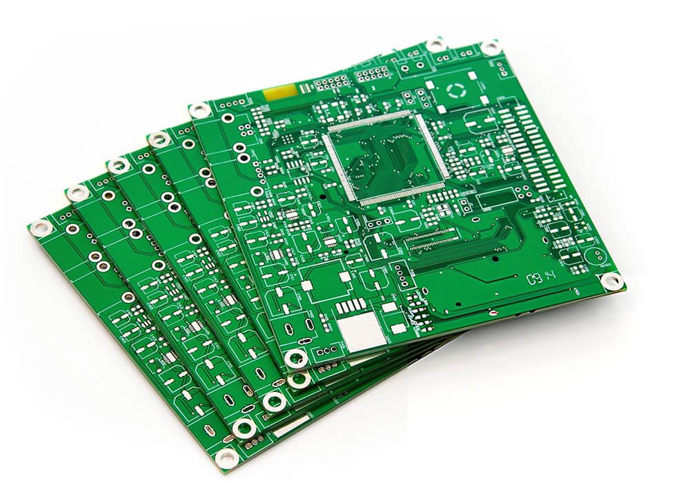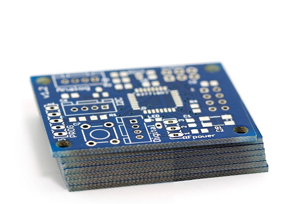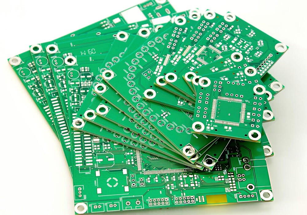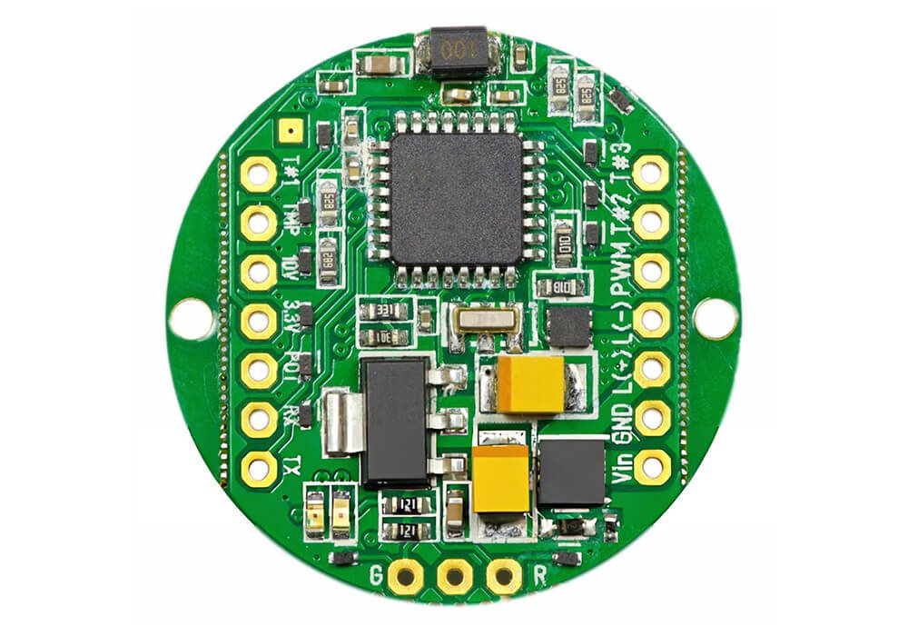


Single- to Multilayer Rigid PCB.

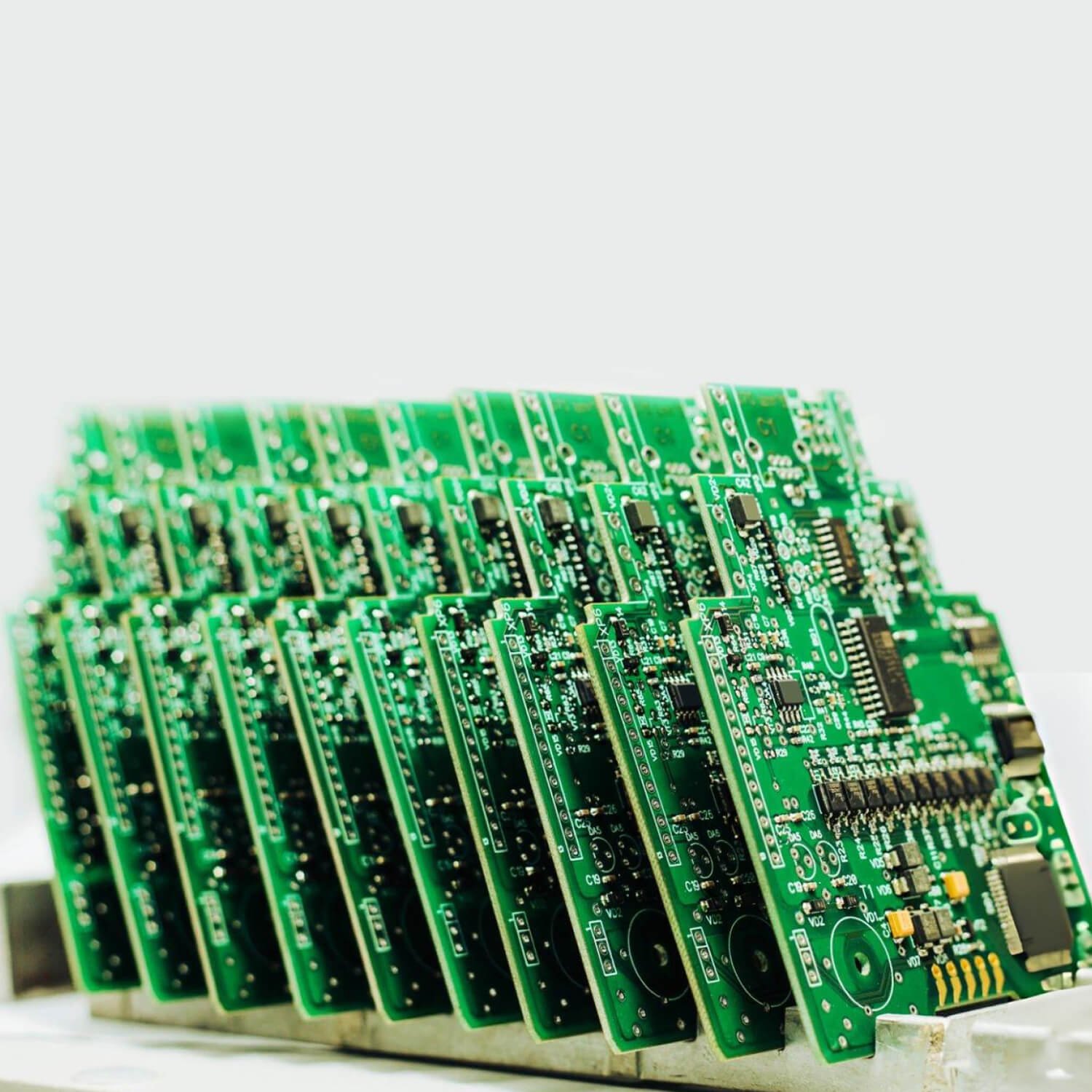
PCBSAIL is specializing in manufacturing of rigid PCBs, from single-sided to 32-layer boards with controlled impedance and heavy copper. We offered end to end service from design review, PCB prototyping, volume production, and turnkey PCB assembly.

Before production, we review your files and confirm materials, tolerances, and testing requirements. Our engineers work with you to resolve manufacturing questions before the boards are built.

Rigid PCB Manufacturing Factory

What Is Rigid PCB?

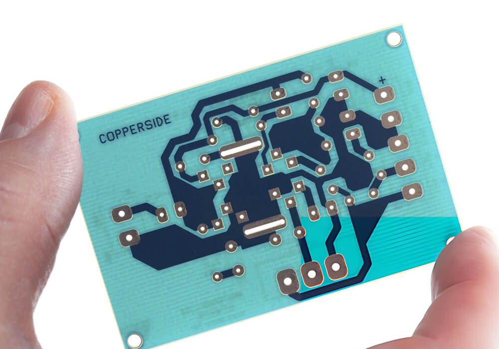
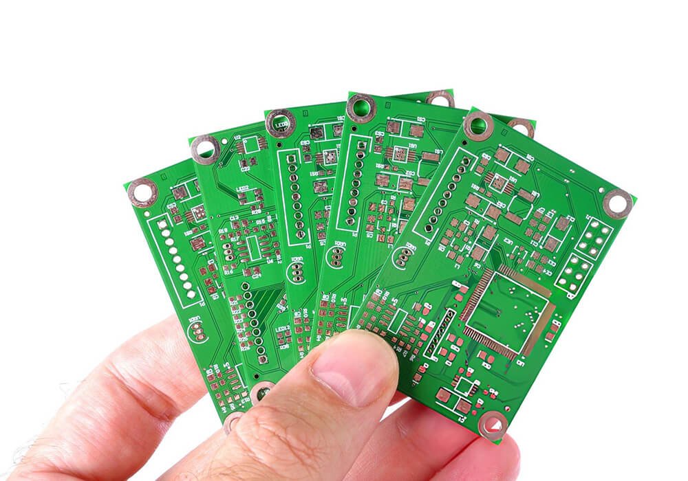
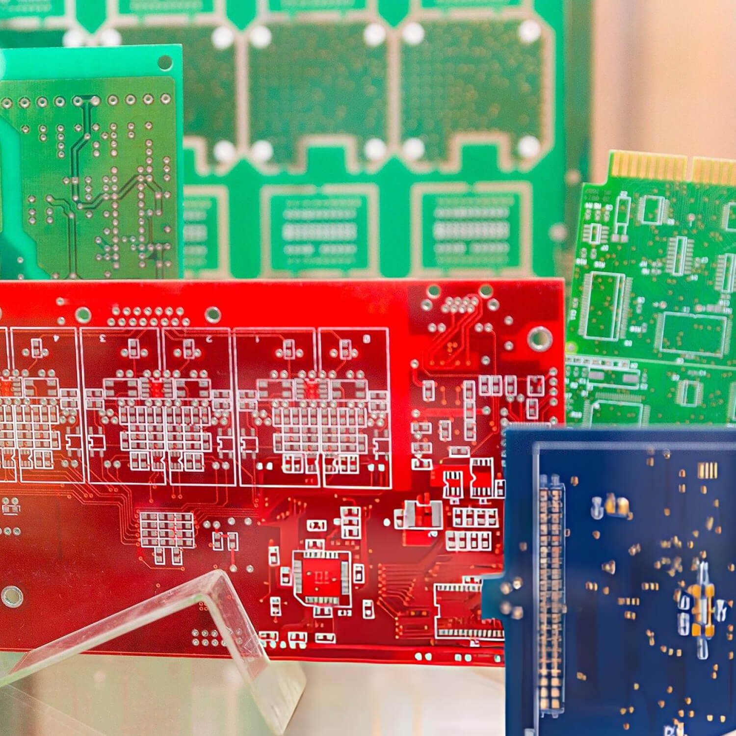
A rigid PCB is a printed circuit board made from a solid substrate, such as fiberglass-reinforced epoxy. Copper tracks connect the components mounted on the board. Rigid PCBs can be single-sided, double-sided, or multilayer.

FR-4, high-Tg FR-4, and halogen-free laminates can be used. Finished board thicknesses from 0.1 to 12 mm can be offered. We support blind and buried vias, gold fingers, controlled impedance, and peelable solder masks, with finishes such as ENIG, lead-free HASL, and immersion silver.

We confirm inspection methods and applicable IPC-6012 Class 2 or Class 3 requirements for each order. AOI, X-ray inspection, and impedance testing are used. RoHS requirements and relevant quality documentation can also be discussed during quotation.

pick and place machine for pcb assembly

Rigid PCB Layer

We manufacture rigid PCBs from 1 to 32 layers. For multilayer boards, we review the stack-up and prepreg selection before vacuum lamination to control layer thickness and alignment.

  • Layer Count: 1–32 layers
  • Constructions: Single-sided, double-sided, multilayer, and HDI
  • Stack-up: Symmetrical and hybrid
  • Interlayer Registration: ±25 μm
  • Dielectric Thickness Tolerance: ±10%

370hr pcb material

Materials

We help you choose materials based on your board’s electrical, thermal, and cost.

  • FR-4: Standard and Ddvanced Grades
  • High Tg Materials: S1000H, IT180, S1150G (Tg 135 °C–180 °C
  • Halogen-free Laminates
  • Metal-core Materials: Aluminum and copper
  • Specialty Materials: High-frequency laminates and mixed-material stack-ups
online pcb manufacturing

Fine-Line & Drilling

We can support compact routing, impedance-controlled traces, and dense pad arrays for advanced rigid PCB designs.

  • Min. trace / spacing: 1.8 mil / 1.8 mil
  • Min. mechanical drill: 0.08 mm
  • Annular ring tolerance: ≥4 mil
  • Imaging: LDI (Laser Direct Imaging)
Feature Rigid PCB.

We provides a comprehensive range of rigid PCB, manufactured with certified materials and IPC-compliant processes to meet different cost, performance, and reliability requirements.

Best Rigid PCB Price
Best Rigid PCB
Cheaper Rigid PCB
pcb company near me
pcb printing near me
pcbs near me

Rigid PCB We Offer.

Flex PCB Single-Sided Flex PCB

Single-Sided Rigid PCB

Single-sided rigid PCBs have one copper layer on an FR-4 or CEM-1 substrate. They are a cost-effective choice for simple circuits.

  • Substrate: FR-4 or CEM-1
  • Finished Board Thickness: 0.1–1.6 mm
  • Copper Weight: 0.5–2 oz
  • Options: Solder mask and silkscreen

Flex PCB Double-Sided Flex PCB

Double-Sided Rigid PCB

There are copper on both sides of Double-Sided Rigid PCB, giving designers more room for routing. Plated through-holes connect the two layers. These boards support both surface-mount and through-hole components.

  • Core Material: FR-4
  • Core Thickness: 0.6–2.0 mm
  • Min. Mechanical Drill Diameter: 0.3 mm Acceptance
  • Requirements: IPC Class 2 or Class 3, as specified
  • Options: Solder mask, via tenting, and silkscreen

Flex PCB Multilayer Flex PCB

Multilayer Rigid PCB

Multilayer rigid PCBs consist of multilayer copper layers, laminated with prepreg and cured under controlled heat and pressure. These stackups integrate signal, power, and ground planes to support high-density interconnects and stable electrical performance.

  • Layer count: 4–32 layers
  • Layer registration: ±25 μm
  • Copper balancing
  • Controlled impedance modeling for high-speed digital and RF circuits

Flex PCB with Stiffeners

High Tg Rigid PCB

High Tg rigid PCBs are made of advanced laminate materials such as S1000H, IT180, and S1150G, with glass transition temperatures above 170 °C. They are designed for lead-free soldering and continuous operation in high-temperature environments.

  • Tg ≥ 170 °C
  • Excellent thermal cycling resistance
  • Available across all layer counts and copper weights
  • Pre-bake processes and extended delamination testing

Flex PCB Rigid-Flex PCB

Rigid-Flex PCB

Rigid-flex PCBs combine rigid FR4 sections with flexible polyimide layers, enabling folding, bending, and compact 3D integration. This structure improves reliability by reducing connectors and interconnect failures.

  • Hybrid rigid + flex stackups
  • Polyimide flex layers with coverlay
  • Flex region thickness: 0.1 mm – 0.5 mm
  • Dynamic bend and endurance testing
  • Controlled drilling and standard copper weights in rigid areas

Flex PCB Rigid-Flex PCB

Metal-Backed Rigid PCB

Metal-backed rigid PCBs (metal core PCBs) use aluminum or copper substrates to enhance heat dissipation and mechanical stability.

They are ideal for high-power and thermally demanding applications.

  • Metal core: Aluminum or copper
  • Core thickness: 0.8 mm – 2.0 mm
  • Dielectric isolation layer
  • 1–3 copper layers laminated above the metal core
Item

Rigid PCB

Max. Layer Count

32 layers

Min. Inner-Layer Trace Width / Spacing

2 / 2 mil

Min. Outer-Layer Trace Width / Spacing

2.5 / 2.5 mil

Inner Layer Max Copper

6oz

Outer Layer Max Copper

6oz

Min. Drilled Hole Diameter

0.20 mm

Min Laser Drilling

0.1mm

Max Aspect Ratio (Mechanical Drilling)

20:01

Max Aspect Ratio (Laser Drilling)

1:01

Press Fit Hole Tolerance

±0.05mm

PTH Tolerance

±0.075mm

NPTH Tolerance

±0.05mm

Countersink Tolerance

±0.15mm

Finished Board Thickness

0.4–8 mm

Typical Impedance Tolerance

Confirm by stack-up

Board Thickness Tolerance(<1.0mm)

±0.1mm

Board Thickness Tolerance(≥1.0mm)

±10%

Min Board Size

10*10mm

Max Board Size

22.5*30 inch

Contour Tolerance

±0.1mm

Min. BGA Pad Diameter (HDI)

0.15 mm

Min SMT

7*10mil

Min Solder Mask Clearance

1.5mil

Min Solder Mask Dam

3mil

Min Legend Width/Height

4/23mil

Strain Fillet Width

/

Bow & Twist

0.003

"Ready To Start Building Your PCB?"

Rigid PCB Materials.

Our Rigid PCB is made of the different substrate materials depending on operating temperature, signal frequency, and mechanical requirements.

Rigid PCB Materials

Copper-clad epoxy glass laminates are made from woven glass cloth bonded with epoxy resin. Its surface was covered with copper foil. It can generally offer better mechanical strength, dimensional stability, and resistance to impact.

FR-4 is widely used for rigid PCBs. FR-5 is another epoxy-glass grade suited to applications that require greater heat resistance.

Key Properties:

  • Dielectric Constant: Typically 4.3–4.9, depending on the material and test frequency
  • Heat Resistance: Depends on the laminate grade and operating conditions
  • Moisture Bbsorption: Generally low
  • Mechanical Support: A strong, stable base for components and copper circuitry

Epoxy glass cloth prepreg is woven fiberglass impregnated with partially cured epoxy resin, known as B-stage resin. It is used to bond layers together in multilayer PCBs.

During lamination, heat and pressure cause the resin to flow and then fully cure. The cured material holds the layers together and electrically insulates the copper layers.

Main Functions:

  • Bond the layers of a multilayer PCB
  • Provide electrical insulation between copper layers
  • Help establish the dielectric thickness needed for controlled impedance

Self-extinguishing copper-clad laminates are PCB materials. It can resist burning and stop burning after the ignition source is removed under specified test conditions. They also provide the mechanical support and electrical insulation needed for the board.

Key Benefits:

  • Help limit continued burning
  • Offer flame-retardant material options for power electronics and enclosed devices
  • Support product safety requirements when the selected grade has the required flame rating

Copper-clad PTFE glass-fiber laminates are compost of a PTFE dielectric with glass-fiber reinforcement. Their low dielectric loss makes them useful for high-frequency and RF circuits where signal loss matters.

Key Properties:

  • Low dielectric constant and loss tangent
  • Good heat resistance
  • Low moisture absorption
  • Good chemical resistance

Metal core PCBs (MCPCBs) use a metal base, usually aluminum or copper.They are designed to move heat away from components more efficiently. It can keep the board cool and stable during working. 

It makes them a good choice for electronics that generate a lot of heat.

Key Benefits:

  • Better heat dissipation: Transfers heat away from components quickly.
  • Greater mechanical strength: Provides a strong and stable base for electronic components.
  • EMI shielding: Helps reduce electromagnetic interference in certain applications.

Rigid PCB Feature.

Our rigid PCBs can holds components in place and keeps the board’s shape during use. Their flat, stable structure makes assembly, inspection, and mounting straightforward.

Our rigid PCBs are made with FR-4, High-Tg, halogen-free, or metal-core materials. They provide a solid, stable base for electronic components and can withstand vibration, impact, and everyday mechanical stress.

Key Features:

  • Rigid structure: Keeps its shape and does not bend during normal use.
  • High mechanical strength: Handles vibration, impact, and physical stress.
  • Dimensional stability: Maintains its shape during assembly and operation.

Our rigid PCBs offer reliable electrical performance for both low-speed and high-speed circuits. They can meet different signal and impedance requirements, such as high-density and high-frequency applications.

Key Features:

  • Stable dielectric properties: Help maintain consistent electrical performance.
  • Controlled impedance: Supports reliable signal transmission in high-speed circuits.
  • Low signal loss: Helps reduce signal loss and unwanted interference.
  • High-density design support: Suitable for compact layouts and high-frequency applications.

Our rigid PCBs are designed to withstand lead-free soldering profiles and continuous operation in elevated temperature environments.

  • High Tg materials available (≥170 °C)
  • Excellent thermal cycling resistance
  • Metal-core options for enhanced heat dissipation

We offer a range of surface finishes to protect rigid PCBs and ensure good solderability during assembly. Each finish is selected based on the board design, component requirements, and intended application.

Available Options:

Rigid PCB Feature

From Your PCB Files to Boards Ready for Assembly.

A straightforward process that keeps you informed, reduces production risks, and gets your PCBs ready for the next stage.

01

Send Us Your PCB Requirements

Share your Gerber or ODB++ files, drawings, order quantity, material preferences, stack-up, and testing requirements. Our team will review your request and confirm the details before moving forward.

02

Review and Confirm Before Production

Our engineering team reviews your design, including material selection, stack-up, trace width and spacing, copper thickness, and impedance requirements. We will contact you if any details need clarification.

03

Get Your Boards Manufactured

Once everything is confirmed, we move your order into production. From material preparation and circuit imaging to drilling, plating, surface finishing, and routing, each step follows the approved specifications.

04

Receive Inspected, Ready-to-Use PCBs

Before shipment, your boards go through the required visual, dimensional, and electrical checks. We then arrange protective packaging and delivery, so your PCBs arrive ready for assembly.

Rigid PCB Manufacturing.

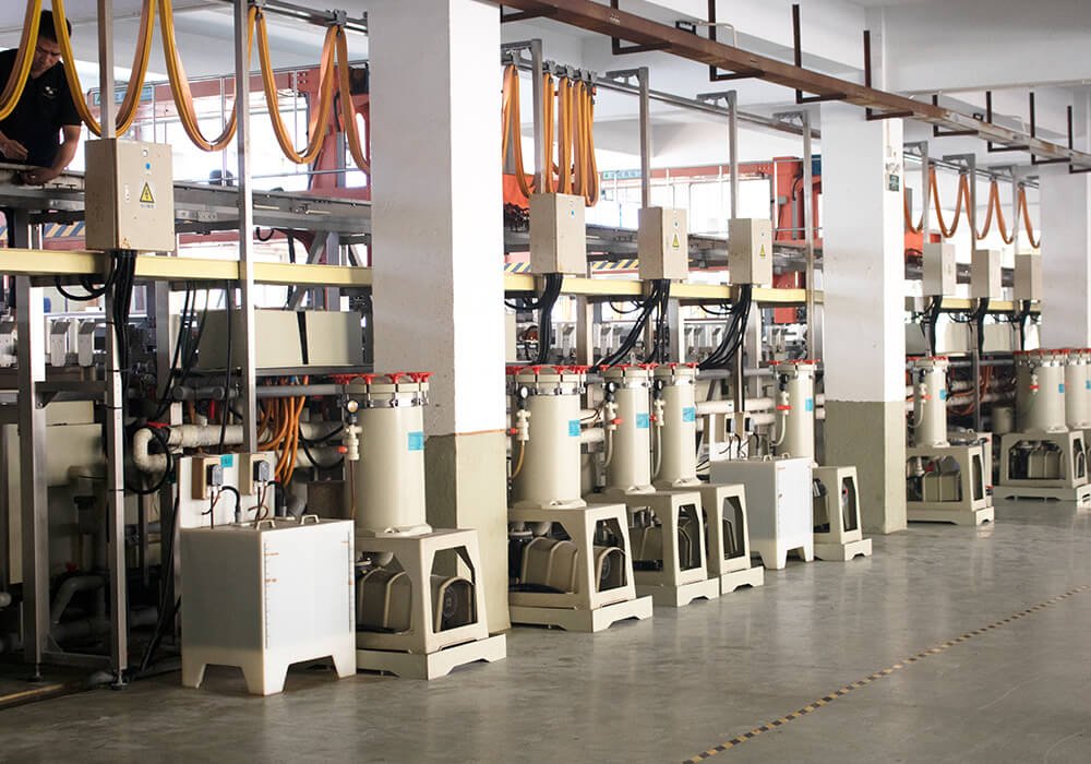
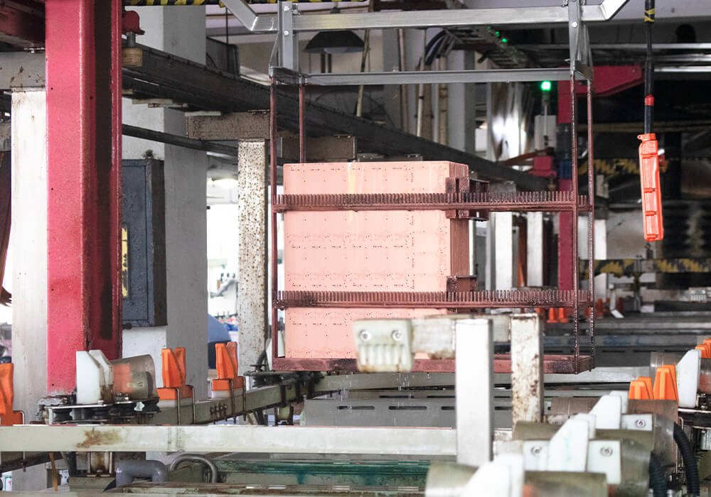
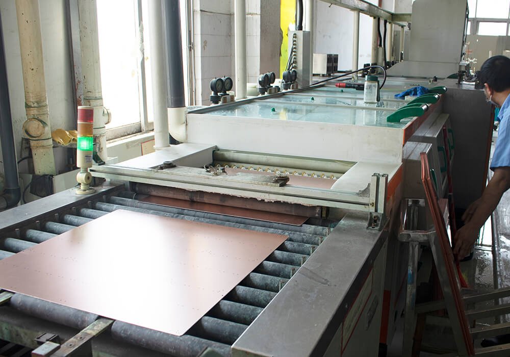
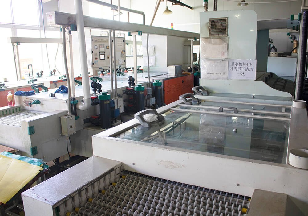
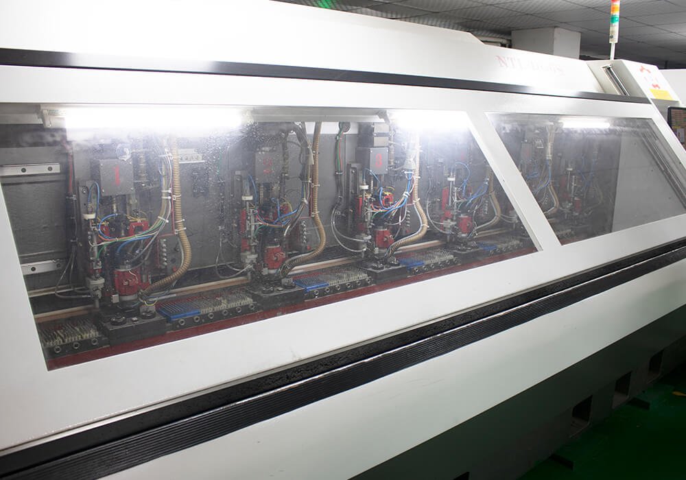
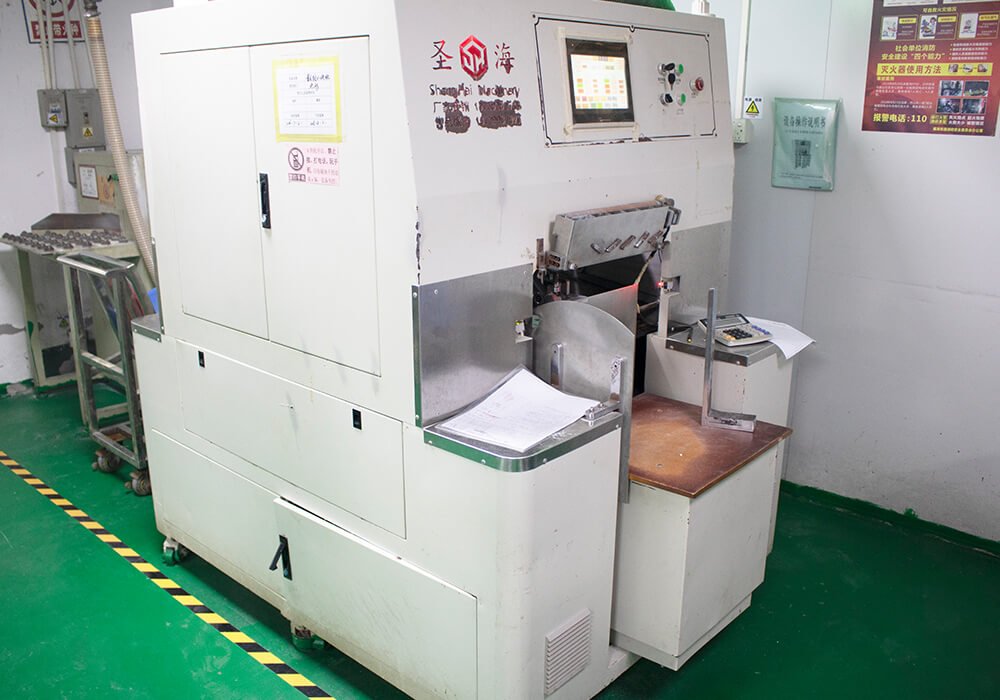
Rigid PCB manufacturing involves several steps, such as material preparation, circuit pattern transfer, etching, drilling, and surface finishing.

We follow controlled production steps and carry out DFM checks before manufacturing. It can identify potential design issues early and ensures the board meets the required specifications for assembly, electrical performance, and reliable operation.

PTH
copper immersion
Degumming Residue
sink gold
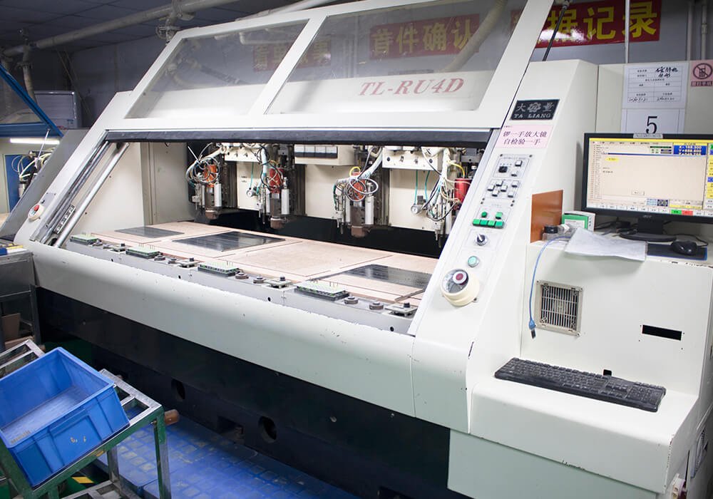
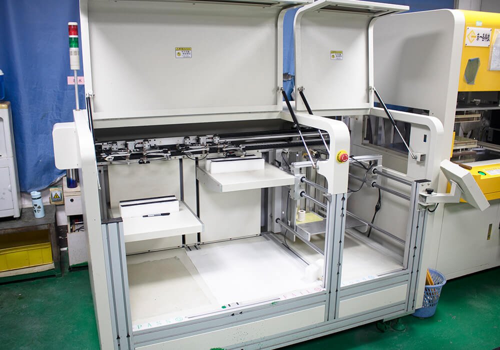
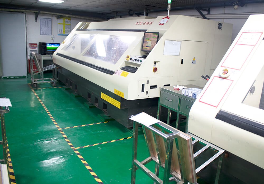
PCB Drill Machine
PcB Manufacturing Machine
Etching
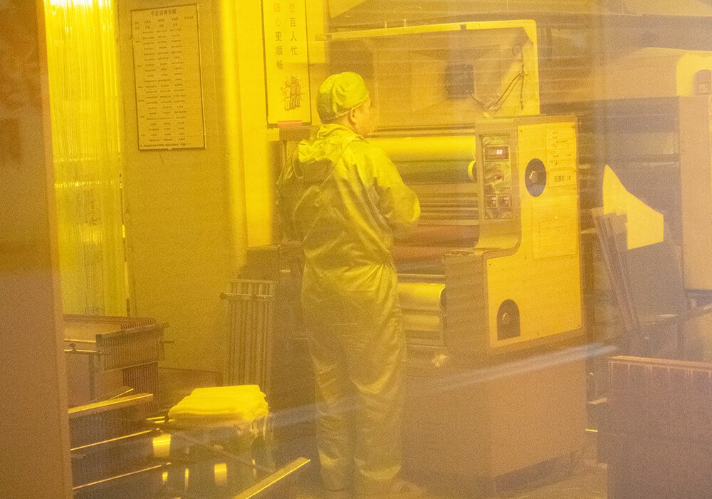
Imaging room
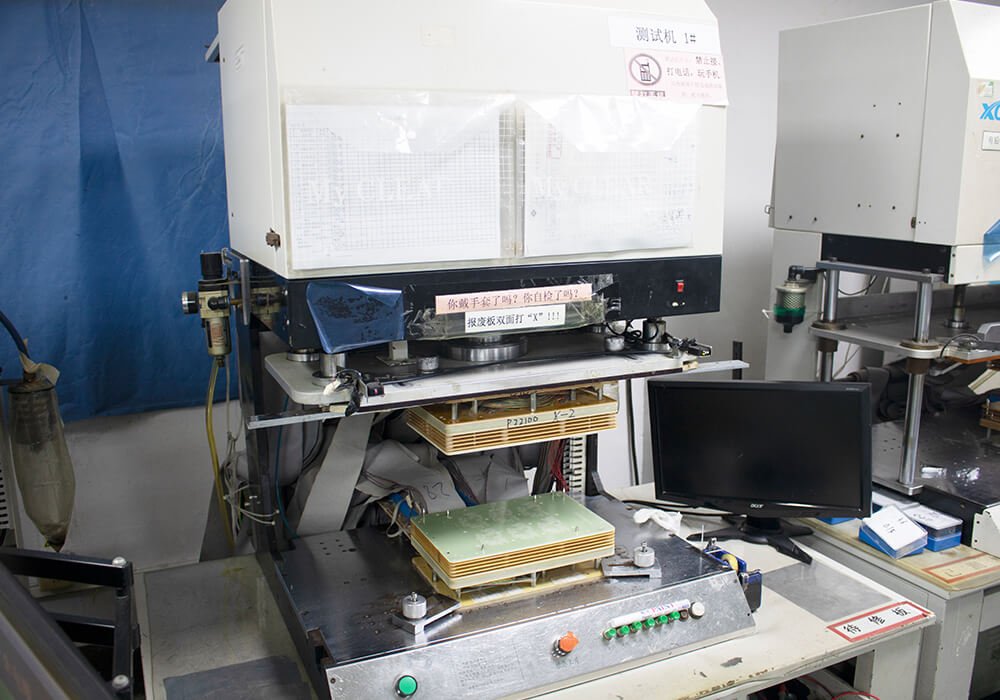
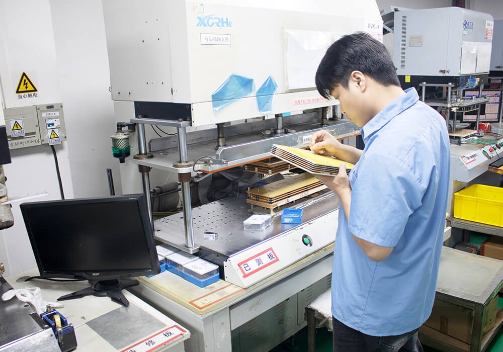
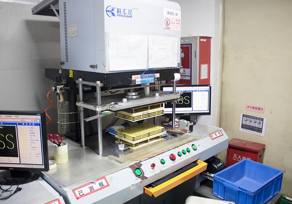
PCB Test Machine
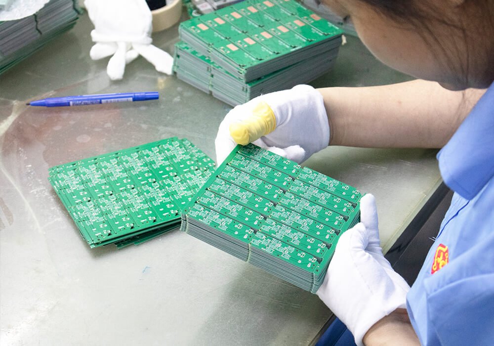
PCB Checking
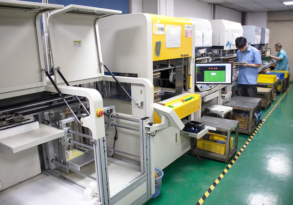
PCB Checking Machine
PCB Chechking
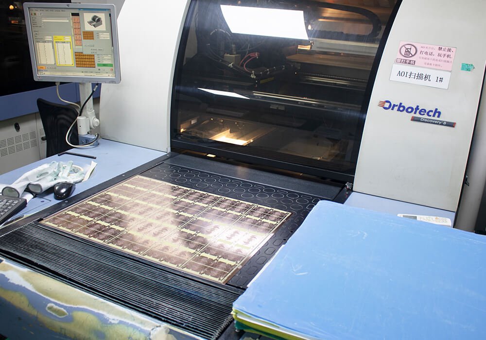
PCB AOI
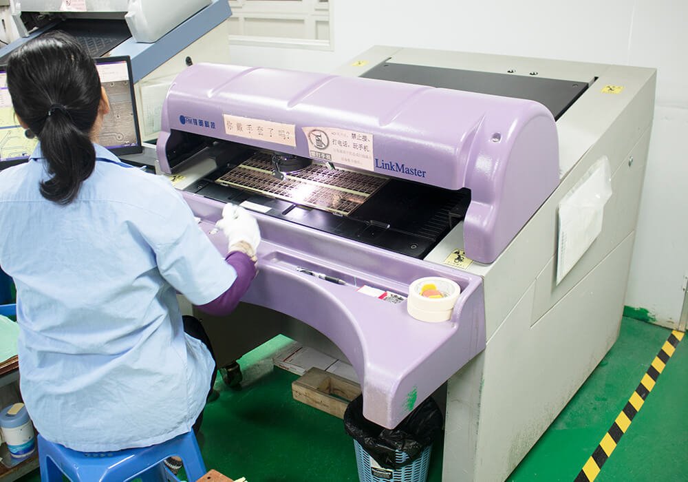
Link Master
Drill Machine
checking machine
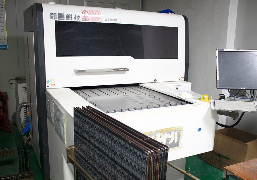
screen printing machine
Eye Checking
Pcb layout example

Circuit Pattern

The PCB layout is first finalized using professional PCB design software. Manufacturing data typically includes:

  • Gerber files
  • Drill files
  • Stack-up and fabrication notes
For prototype or low-volume production, the circuit pattern is transferred onto a photosensitive or resist-coated copper-clad laminate using high-resolution imaging methods. Proper orientation and alignment are critical to ensure dimensional accuracy.

PCB layout software

Copper-Clad Laminate

A copper-clad laminate consists of an insulating substrate—commonly FR4—with copper foil laminated to one or both sides. The laminate is:

  • Cut to the required board size
  • Cleaned and surface-prepared to remove oxidation

Surface conditioning improves resist adhesion and ensures clean, well-defined copper traces during subsequent processing.

pcb design online free

Preprocessing & Circuit Transfer

Before pattern transfer, the copper surface is lightly treated to eliminate oxidation and contaminants.

The circuit image is then transferred onto the copper surface using:

  • Thermal transfer (for basic prototyping), or
  • Photoresist exposure and imaging (for production-grade PCBs)

Precise alignment ensures trace geometry, pad placement, and edge clearance meet design specifications.

smt assembly machines

Circuit Etching

After transfer, exposed copper areas are removed using a controlled chemical etching process, leaving behind the desired conductive pattern. Key controls during etching:

  • Uniform copper removal
  • Consistent trace width
  • No undercutting or over-etching
Any incomplete transfer areas are corrected prior to etching to prevent open circuits or signal integrity issues.

pcb design online free

Drilling & Hole Preparation

Once the circuit pattern is defined, holes are drilled for:

  • Through-hole components
  • Vias
  • Mechanical mounting
Drilling accuracy is essential for reliable solder joints and plated interconnections in multilayer designs. After drilling:
  • Residual resist or toner is removed
  • Hole walls are cleaned to prepare for plating or soldering

pcb assembly failure

Board Finishing & Assembly

ollowing drilling, the PCB undergoes final surface preparation steps, including:

  • Cleaning and surface conditioning
  • Flux or protective coating application (if required)

At this stage, the PCB is ready for component soldering, either manually (for simple prototypes) or via automated SMT/THT assembly in production environments.

fr 4 pcb design

DFM Verification

Before volume manufacturing or assembly, DFM analysis is performed to identify and eliminate potential issues such as:

  • Insufficient trace spacing
  • Poor solderability
  • Inadequate pad sizes
  • Thermal imbalance
DFM ensures the PCB can be manufactured efficiently, assembled reliably, and perform as intended in real-world applications.

Rigid PCB Quality Control and Testing.

In our factory, every rigid PCB goes through a series of quality checks to make sure it meets your design requirements before shipment. From visual inspection to electrical testing, we check the details that matter for reliable assembly and long-term performance.

PCB Chechking

Visual Inspection

Checks for scratches, copper defects, solder mask issues, and other visible problems.

AOI

Detects circuit pattern defects, such as open circuits, shorts, and missing copper.

Electrical Testing

Uses flying probe or fixture testing to check circuit continuity and isolation.

Dimensional Inspection

Verifies board thickness, hole sizes, dimensions, and tolerances.

Impedance Testing

Confirms controlled impedance meets the specified requirements.

Microsection Analysis

Examines internal layer alignment, copper thickness, plating quality, and via structure.

Rigid PCB Applications.

Our Rigid PCBs are the most widely used in modern electronics due to their mechanical strength, dimensional stability, electrical performance, and cost efficiency.

PCB Manufacturer Industrial Automation

Industrial Control

Rigid PCBs are extensively used in industrial control systems where long-term reliability and resistance to vibration are critical. Typical applications

  • PLC control boards
  • Motor drive and inverter PCBs
  • Industrial power supplies
  • Sensors and I/O modules

PCB Manufacturer Automotive Electronics

Automotive Electronics

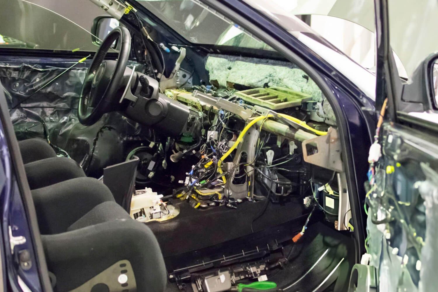
Automotive systems demand high-temperature tolerance, vibration resistance, and long service life. Rigid PCBs are essential in both conventional and electric vehicles. Typical applications

  • Engine control units (ECU)
  • Battery management systems (BMS)
  • ADAS control modules
  • Power distribution units

PCB Manufacturer Consumer Electronics

Consumer Electronics

Rigid PCBs form the core of mass-produced electronic products due to their low cost and scalability. Typical applications

  • Smartphones and tablets
  • Home appliances
  • Audio and video devices
  • Smart home electronics
  • Portable juice blender
PCB Manufacturer Power Electronics

Power Electronics

Rigid PCBs are widely used in power conversion and energy control systems, especially when heavy copper or metal cores are required.

Typical applications

  • Power converters
  • Inverters
  • Solar energy controllers
  • EV charging systems

PCB Manufacturer Medical Devices

Medical Electronics

Medical devices require high reliability, precision, and regulatory compliance. Rigid PCBs are commonly used in diagnostic and monitoring equipment.

Typical applications

  • Patient monitoring systems
  • Diagnostic imaging equipment
  • Laboratory analyzers
  • Medical control units
PCB Manufacturer LED Lighting

LED Lighting

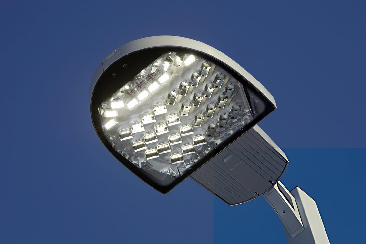
Metal-core and rigid PCBs are essential for efficient thermal management in LED lighting.

Typical applications

  • High-power LED modules
  • Automotive LED lighting
  • Industrial lighting systems

Fast Quotation.

Our professional sales and engineering teams provide fast PCB quotes and technical support. Simply send us your Gerber files, BOM, and assembly drawings, and we will respond promptly with a competitive solution.

FAQ About Rigid PCB

1. What Is A Rigid PCB

A rigid PCB (Rigid Printed Circuit Board) is a traditional printed circuit board made from solid, non-flexible substrate materials, most commonly FR4 epoxy glass laminate.
Rigid PCBs provide excellent mechanical stability, electrical performance, and long-term reliability, and they are widely used in consumer, industrial, automotive, and medical electronics.

Common rigid PCB materials include:

  • FR4 (standard epoxy glass laminate)
  • High-Tg materials (S1000H, IT180, S1150G)
  • Halogen-free laminates
  • Metal core materials (aluminum or copper core)

Material selection depends on temperature, electrical, and mechanical requirements.

PCBSAIL manufactures rigid PCBs from 1 to 64 layers, including:

  • Standard multilayer stack-ups
  • HDI structures
  • Controlled impedance designs

Rigid PCB thickness typically ranges from:

  • 0.1 mm to 12.0 mm

Standard thicknesses include 0.8 mm, 1.0 mm, 1.6 mm, and custom builds are supported for special applications.

Copper thickness options range from:

  • 0.33 oz to 28 oz per layer

Heavy copper rigid PCBs are used in power electronics, automotive systems, and high-current applications.

PCBSAIL offers multiple surface finishes:

  • ENIG
  • HASL / Lead-Free HASL
  • OSP
  • Immersion Silver
  • Immersion Tin

All finishes are RoHS compliant and compatible with lead-free assembly.

  • IPC Class 2: Standard reliability for consumer and commercial electronics
  • IPC Class 3: High-reliability level for automotive, medical, military, and aerospace applications

Class 3 PCBs have stricter requirements for plating thickness, annular ring, and inspection.

Yes. High-Tg rigid PCBs are designed to withstand:

  • Repeated lead-free soldering cycles
  • Continuous operating temperatures above 130°C

Materials with Tg ≥170°C and Td >340°C are commonly used.

Yes. PCBSAIL supports:

  • Single-ended and differential impedance control
  • Impedance modeling and testing
  • High-speed digital and RF rigid PCB designs

PCBSAIL supports minimum trace/spacing of:

  • 1.8 mil / 1.8 mil

This enables dense routing for compact and high-performance designs.

Testing includes:

  • AOI (Automated Optical Inspection)
  • X-ray inspection
  • Electrical testing (flying probe or fixture)
  • Impedance testing (when required)

Class 3 boards may also undergo microsection and thermal shock testing.

Yes. PCBSAIL supports:

  • Rigid PCB prototyping
  • Small-batch production
  • High-volume manufacturing

Fast turnaround options are available, including 24-hour express service.

Yes. PCBSAIL provides one-stop PCBA services, including:

  • PCB fabrication
  • Component sourcing
  • SMT and THT assembly
  • Functional testing

Required manufacturing files typically include:

  • Gerber files (RS-274X)
  • NC drill files
  • PCB stack-up details
  • Fabrication notes

Assembly files are required for PCBA orders.