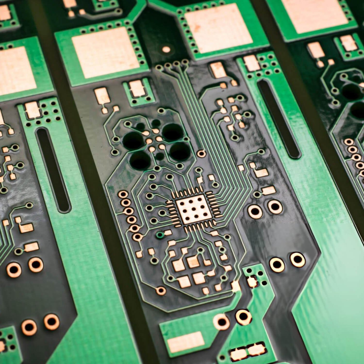
High-Speed PCB.

PCBSAIL provides high-speed PCB fabrication and board assembly for advanced electronic systems. Our manufacturing capabilities support designs for data rates ranging from 25 Gbps NRZ to 112 Gbps PAM4 SERDES architectures.

We use carefully planned PCB stackups, low-loss laminates, and advanced via structures to meet demanding signal transmission requirements in multilayer boards.

From telecommunications equipment to aerospace communication systems, we supports high-speed PCB projects from PCB prototypes through volume production.

High-Speed PCB Manufacturer

What Is High-Speed PCB?

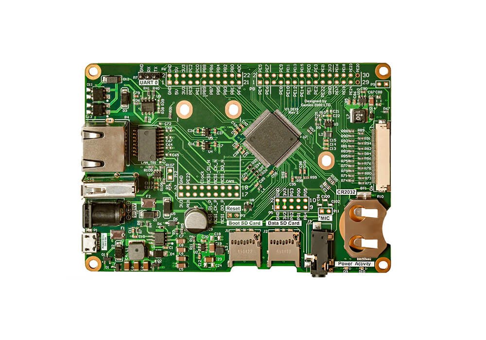
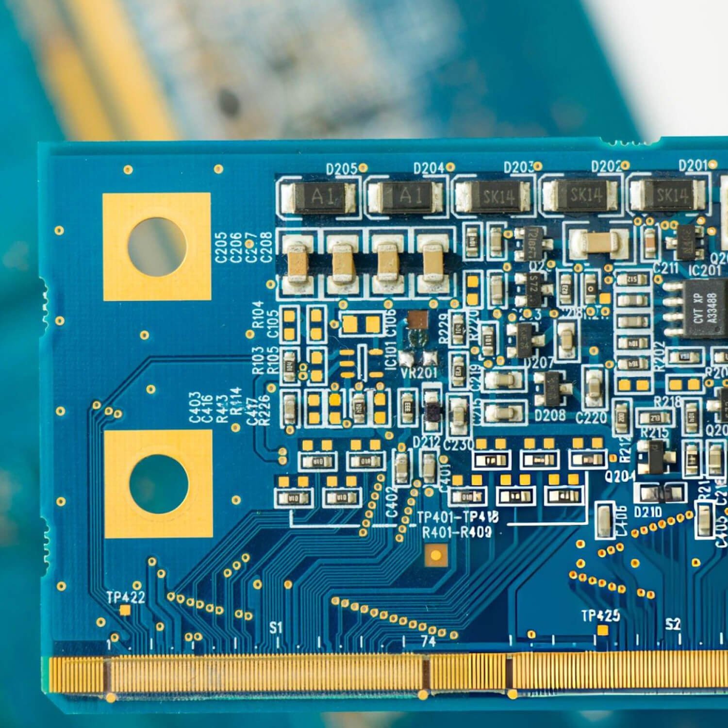
High-Speed PCB is a printed circuit board which is designed to carry high-speed digital signals while maintaining signal quality and timing accuracy. It is used in electronic systems where signals switch very quickly and even small delays, noise, or interference can affect performance.

High-speed PCBs need to carefully control of signal paths, impedance, crosstalk, and electromagnetic interference (EMI). Material selection and PCB stack-up design also play an important role in maintaining signal integrity.

Common Materials for High-Speed PCBs:
Material selection affects signal loss, dielectric constant (Dk), and overall signal performance.

  • Isola High-Speed Materials: For high-speed digital designs that need controlled dielectric properties and low signal loss.
  • Panasonic Megtron 6: For high-speed communication and networking equipment where signal loss needs to be controlled.
  • Rogers Materials: For designs that require specific dielectric properties and stable electrical performance.
  • Nelco Materials: In multilayer and high-speed designs with demanding electrical and thermal requirements.

During engineering review and production, we focus on impedance control, insertion loss, and signal integrity. We also consider S-parameter performance to help ensure predictable electrical behavior at high data rates.

best pcb design software

Manufacturing Equipment

We invests continuously in advanced manufacturing equipment to support high-speed PCB production.

  • Laser Direct Imaging Systems
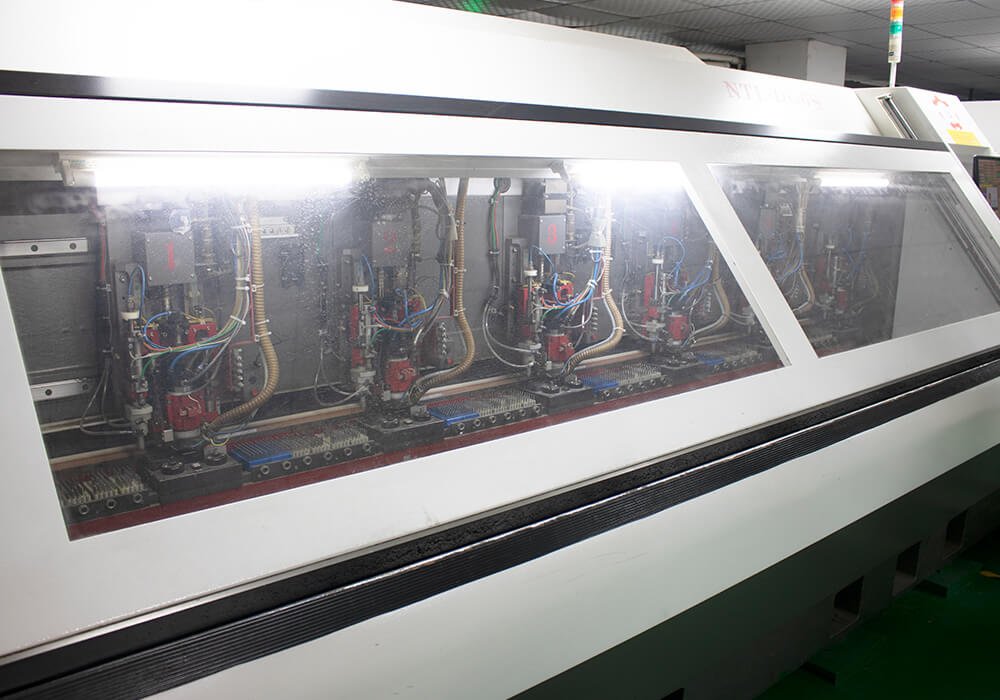
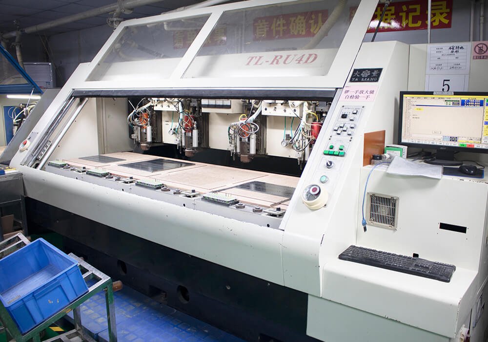
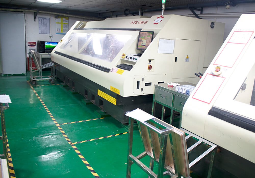
  • High-speed CNC Drilling Systems
  • Laser Drilling for Microvias
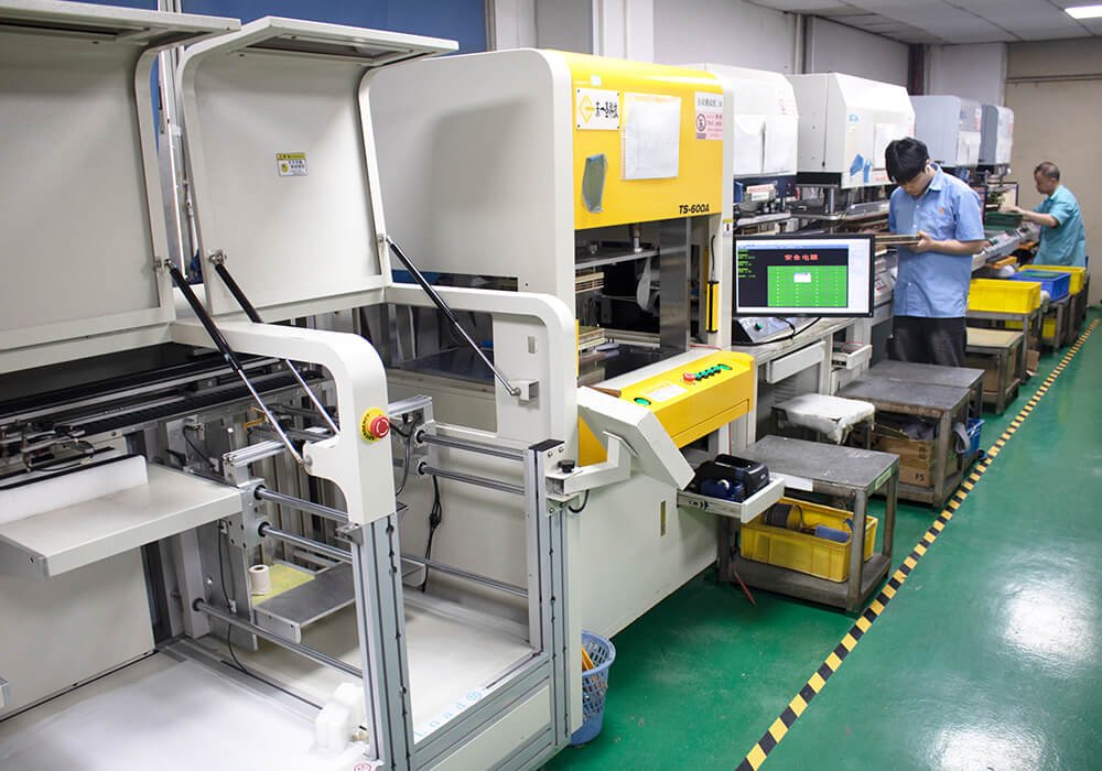
  • Automated Optical Inspection (AOI)
top 10 pcb manufacturing companies in india

Expertise

Our engineering team has extensive experience supporting designs operating from multi-gigabit SERDES links to high-frequency RF systems.

  • Controlled Impedance Stackup Design
  • Differential Pair Routing Strategies
  • Crosstalk And EMI Reduction
  • Return Path Optimization
  • Via Transition Design And Stub Removal
pcb material name

Quality Control

We keep strict quality control through:

  • Incoming Material Inspection
  • AOI Inspection
  • X-ray Inspection
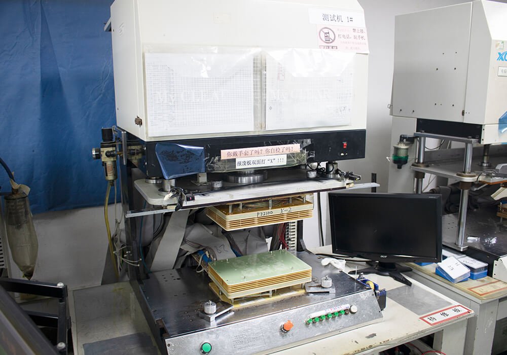
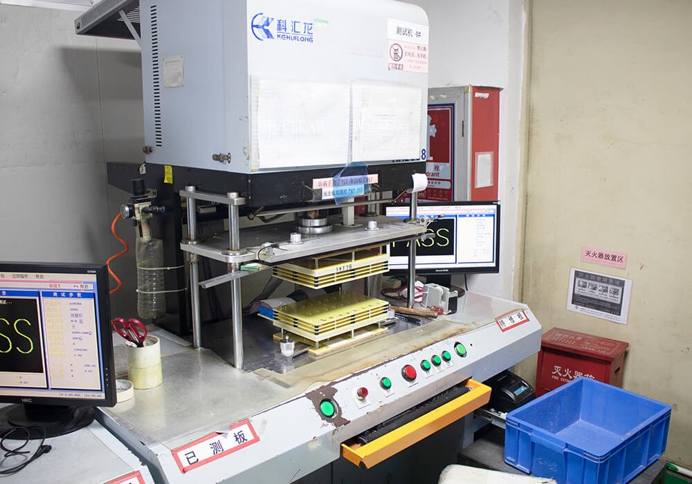
  • Electrical Testing

Feature High-Speed PCB.

We offer a wide range of high-speed PCBs to support different electrical and mechanical requirements.

Best High-Speed PCB
High-Speed PCB Near Me
High-Speed PCB Supplier

High-Speed PCB We Offer.

Flex PCB Single-Sided Flex PCB

Hybrid High-Speed Multilayer PCB

Hybrid stackups combine low-loss laminates near high-speed signal layers with standard FR-4 materials for power or logic layers. It balances performance with cost efficiency.

  • Low-Loss Cores Around SERDES Layers
  • Standard FR-4 For Non-Critical Layers
  • Controlled Impedance Routing
  • Reduced Material Cost

Flex PCB Double-Sided Flex PCB

Full Low-Loss High-Speed PCB

Full low-loss stackups use advanced materials throughout the PCB structure. Typical Materials:

  • Megtron 6
  • Tachyon 100G
  • Isola I-Speed
  • Other ultra-low-loss laminates
These materials offer extremely low dissipation factor (Df) and stable dielectric constant (Dk), allowing high-speed links to operate at 56–112 Gbps with minimal signal degradation.

Flex PCB Multilayer Flex PCB

High-Speed Backplane PCB

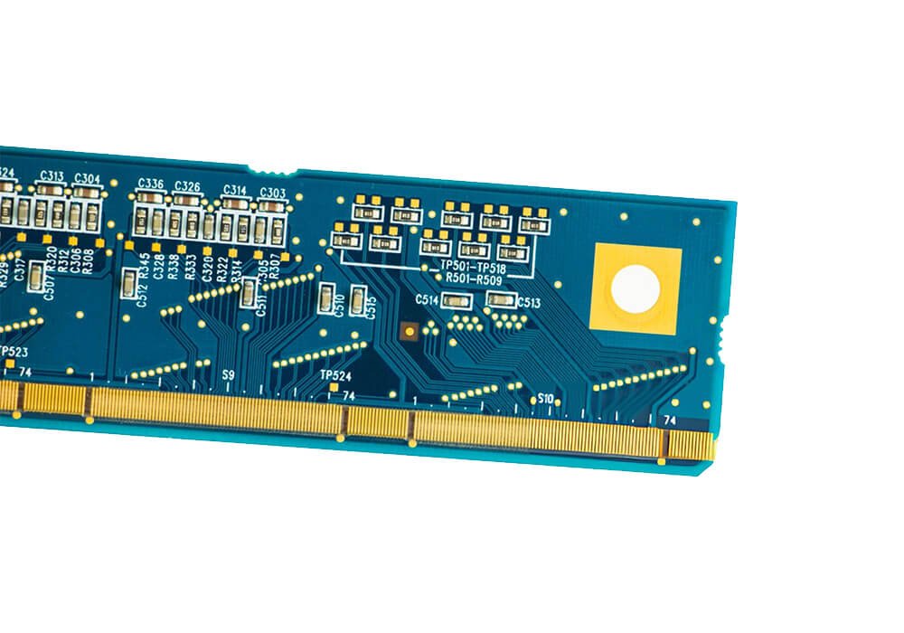
Backplane PCBs are extremely complex multilayer boards designed to interconnect multiple high-speed modules.

  • 20+ Layers
  • Dual Stripline Routing
  • Multi-Depth Back-Drilling
  • Press-Fit Connectors
  • Large Copper Power Planes

Flex PCB with Stiffeners

High-Speed Rigid-Flex PCB

Rigid-flex high-speed PCBs combine rigid board sections with flexible circuits to connect modules in compact enclosures.

  • Reduced Connectors
  • Improved Signal Integrity
  • Space-Saving System Architecture

Flex PCB Rigid-Flex PCB

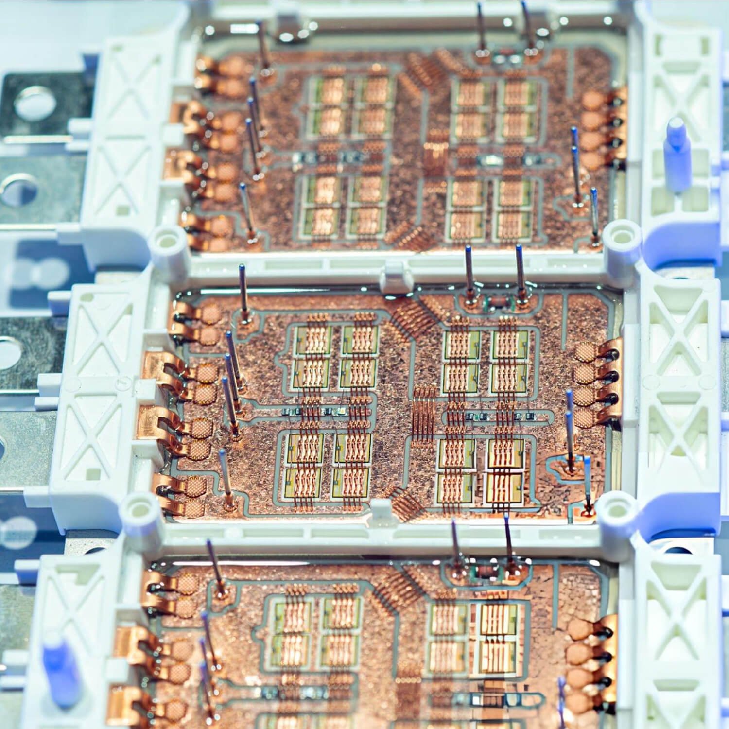
RF / Microwave Hybrid PCB

These PCBs integrate RF materials such as PTFE or hydrocarbon laminates with standard digital PCB layers.
Parameter

Capability

Layer Count

32

Base Materials

Isola I-Speed, RO4350B

Board Thickness

0.8–2.4 mm (zero point eight to two point four)

Copper Weight

0.5–2 oz (zero point five to two ounces)

Min Trace/Space

75/75 μm (3/3 mil; seventy-five by seventy-five micrometers)

Dielectric Constant (Dk)

3.0–4.5 (three point zero to four point five)

Loss Tangent (Df)

<0.005 @10 GHz (less than zero point zero zero five at ten gigahertz)

Impedance Control

±10% (plus/minus ten percent)

Surface Finish

ENIG, Immersion Silver

Quality Testing

TDR, AOI, E-Test

Certifications

ISO 9001, UL, IPC Class 3

Lead Time

7–15 days (seven to fifteen days)

"Ready To Start Building Your PCB?"

Engineering Solutions for High-Speed PCB Design and Fabrication.

We provides comprehensive engineering solutions for high-speed PCB design and fabrication. With advanced material science, signal integrity modeling, controlled impedance manufacturing, and precision fabrication processes, we ensure consistent electrical performance from prototype through volume production.

Engineering Solutions for High-Speed PCB Design and Fabrication

A well-designed stackup is the foundation of every high-speed PCB. Stackup configuration determines impedance control, signal delay, crosstalk behavior, and electromagnetic compatibility.

Key Stackup Design Considerations

  • Controlled Dielectric Thickness
  • Balanced Copper Distribution
  • Reference Plane Placement
  • Symmetrical Lamination Structure
  • Differential Pair Impedance Targets

High-speed PCBs require laminates with stable dielectric properties across a wide frequency range. We support advanced materials designed for high-frequency signal transmission.

Common High-Speed PCB Materials Include:

  • Panasonic Megtron Series Laminates
  • Tachyon High-Speed Materials
  • Isola I-Speed Laminates
  • Hybrid FR-4 / Low-Loss Stackups

Signal integrity is the most important design challenge in high-speed PCB systems. As signal speeds increase, factors such as reflections, crosstalk, and insertion loss can severely impact system performance.

PCBSAIL applies advanced signal integrity techniques to maintain clean high-speed signal transmission.

Controlled Impedance Routing

High-speed differential signals require precise impedance control. Typical impedance targets include:

  • 85 Ω differential for high-speed memory
  • 90 Ω differential for USB and PCIe
  • 100 Ω differential for Ethernet and SERDES

Our controlled impedance manufacturing process maintains tolerance within ±5%.

Differential Pair Routing

Differential pair routing improves noise immunity and signal quality. Our engineering rules include:

  • Tight pair spacing control
  • Length matching
  • Symmetrical routing structures
  • Minimal via transitions

Crosstalk Reduction

High-speed signals routed close together may couple energy and interfere with each other. PCBSAIL mitigates crosstalk through:

  • Ground reference planes
  • Guard traces
  • Proper trace spacing
  • Via stitching techniques

Via structures significantly influence signal quality in high-speed PCBs. Improperly designed vias introduce impedance discontinuities that cause reflections and signal degradation.

PCBSAIL uses multiple via optimization techniques to improve signal performance.

  • Back-Drilled Vias

Back-drilling removes unused portions of plated through holes (PTHs) that act as signal stubs.

Back-drilling is especially important for SERDES channels operating above 25 Gbps.

  • VIPPO (Via-In-Pad Plated Over)

VIPPO technology allows vias to be placed directly in component pads.

  • Microvia Technology

Laser-drilled microvias enable high-density routing and improved electrical performance.

These structures help connect dense BGA layers while maintaining controlled impedance.

High-speed signals require precise timing alignment between signal pairs. Any mismatch in trace length can introduce skew and degrade data integrity.

  • Pair Length Tolerance Within 5–10 Mils
  • Minimal Skew Across High-Speed Channels

High-speed digital systems require stable power delivery to support fast switching components.

Our engineer optimizes the Power Distribution Network (PDN) to reduce noise and maintain voltage stability.

A properly designed PDN prevents issues such as:

  • Ground bounce
  • Voltage droop
  • Power supply noise

High-Speed PCB Feature.

Our high-speed PCBs are engineered to maintain signal integrity, impedance stability, and electrical reliability across complex multilayer structures and high data-rate applications.

We support a wide range of low-loss and ultra-low-loss laminates specifically designed for high-frequency signal transmission.

  • Low Dielectric Loss (Df) For Reduced Signal Attenuation
  • Stable Dielectric Constant (Dk) Across Wide Frequency Ranges
  • Improved Signal Propagation Distance
  • Excellent Thermal Stability

We provided tight impedance control within ±5% tolerance, ensuring stable signal transmission across differential pairs and transmission lines.

All boards are verified through Time Domain Reflectometry (TDR) testing to confirm compliance with design specifications.

We use Very Low Profile (VLP) and Hyper Very Low Profile (HVLP) copper foils to reduce conductor loss and improve signal transmission.

  • Reduced Insertion Loss
  • Improved Signal Reach
  • Enhanced High-Frequency Performance

Our high-speed PCBs are designed to support demanding electronic systems where signal integrity and reliability are critical. Our manufacturing processes ensure consistent electrical characteristics, enabling reliable operation in high-speed environments.

High-Speed PCB Feature

From Your PCB Files to High-Speed PCB Boards Ready for Assembly.

Our process takes your high-speed PCB design from engineering review to finished boards, with careful attention to signal integrity and manufacturing quality.

01

Send Us Your PCB Requirements

Send us your Gerber files and design specifications. Our engineers review the layer stackup, impedance requirements, materials, and signal routing to identify potential issues.

02

DFM Review & Quotation

We check trace widths, spacing, via structures, and manufacturing requirements. After confirming the details, we provide a quotation and estimated lead time.

03

High-Speed PCB Fabrication

Once approved, we start production. Key processes include inner-layer imaging, lamination, precision drilling, copper plating, and surface finishing.

04

Electrical Testing & Delivery

We perform electrical testing and visual inspection to check the finished boards against your specifications. Impedance testing and other checks are carried out where required. Qualified boards are packed and shipped, ready for assembly.

High-Speed PCB Manufacturing.

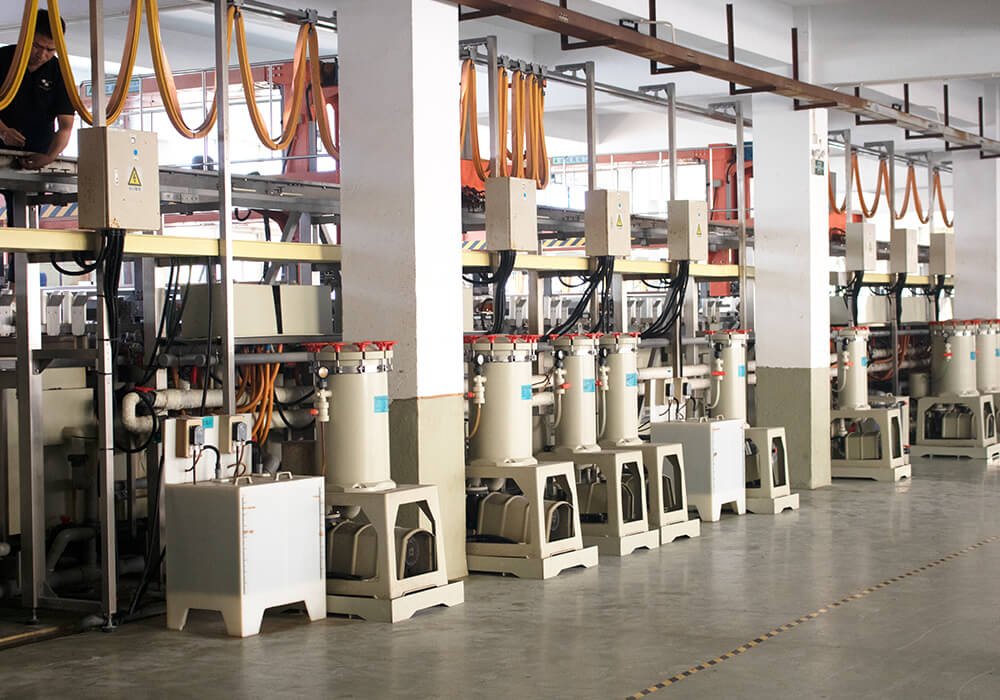
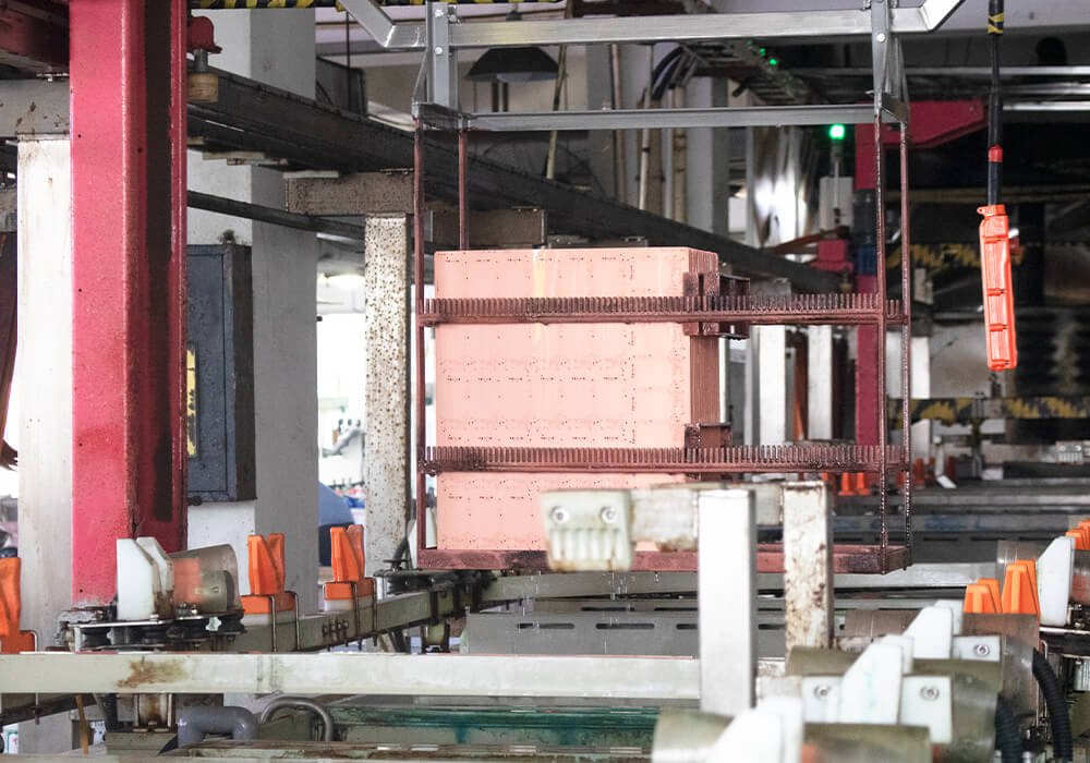
Our high-speed PCB manufacturing process includes carefully selected materials, precise imaging, controlled lamination, and thorough electrical testing.

At every stage, we focus on impedance control, low insertion loss, and consistent signal performance to ensure reliable results from one production batch to the next.

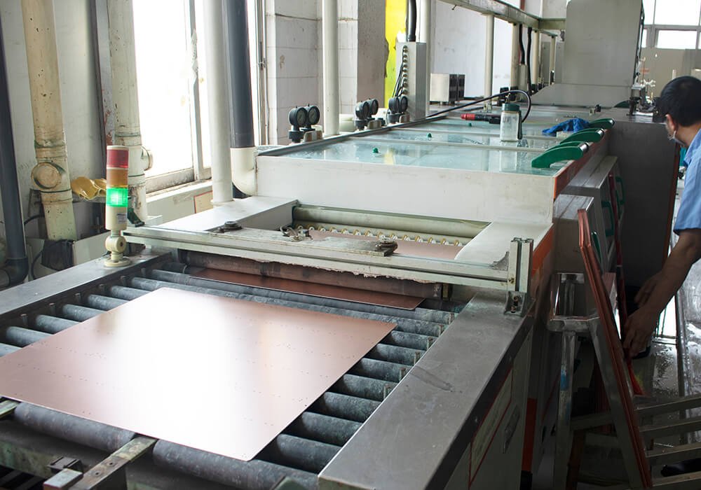
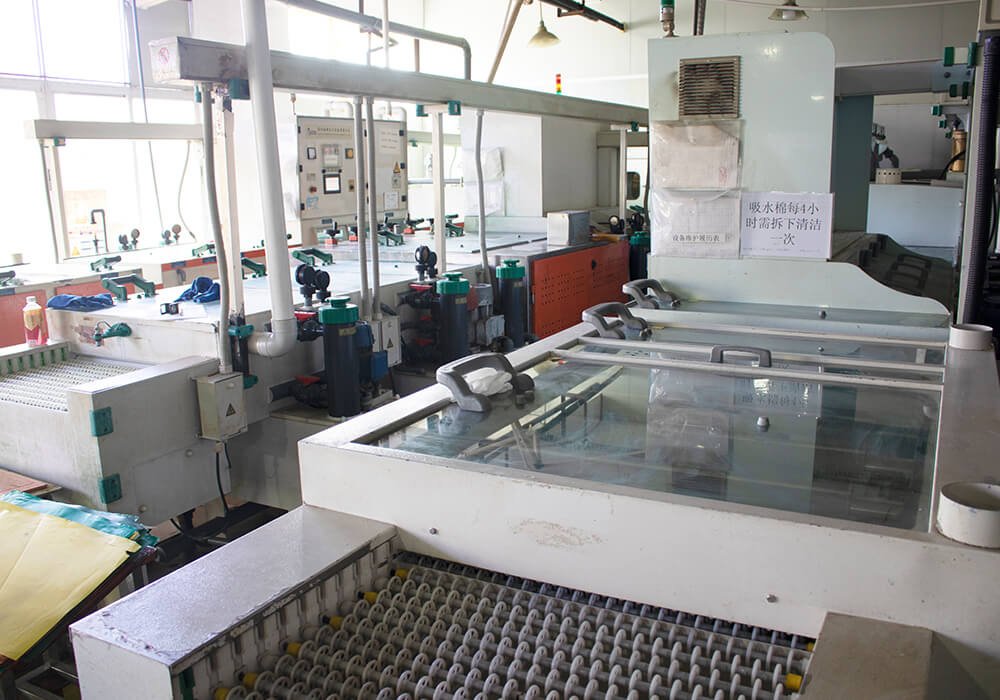
PTH
copper immersion
Degumming Residue
sink gold
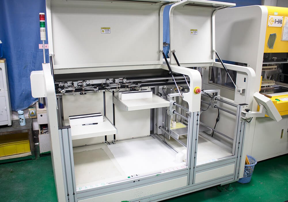
PCB Drill Machine
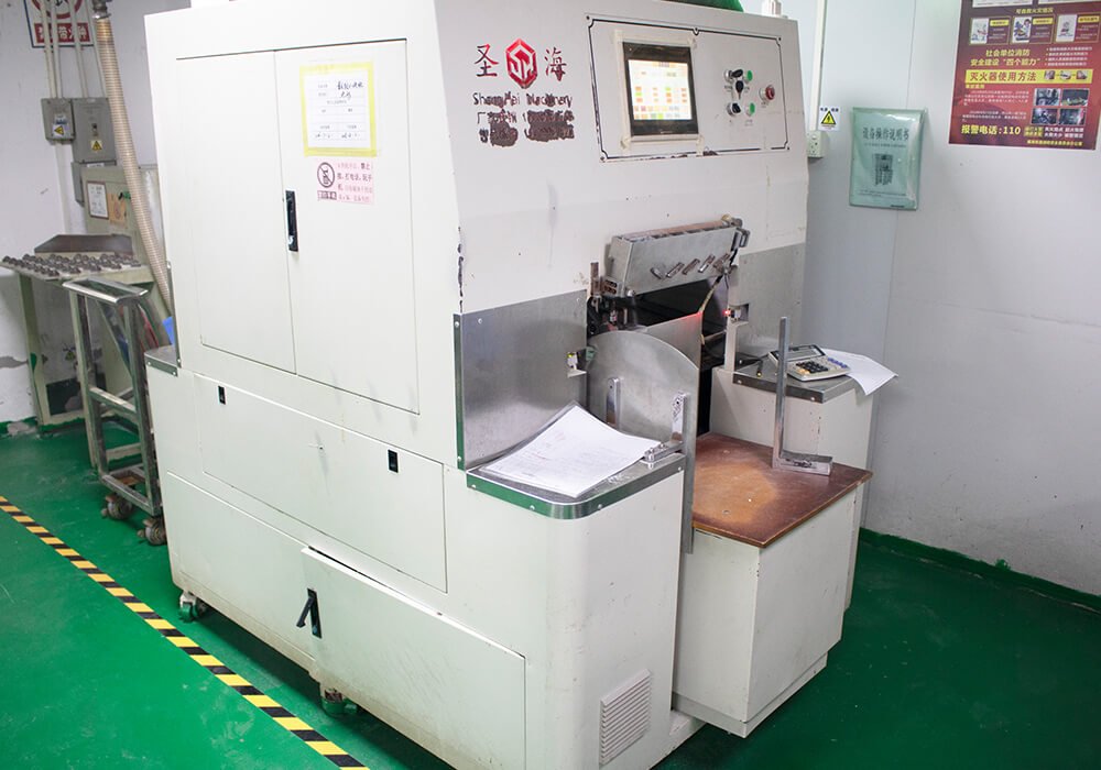
PcB Manufacturing Machine
Etching
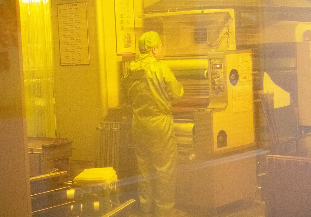
Imaging room
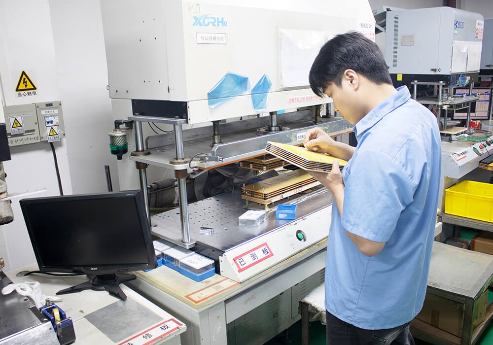
PCB Test Machine
PCB Checking
PCB Checking Machine
PCB Chechking
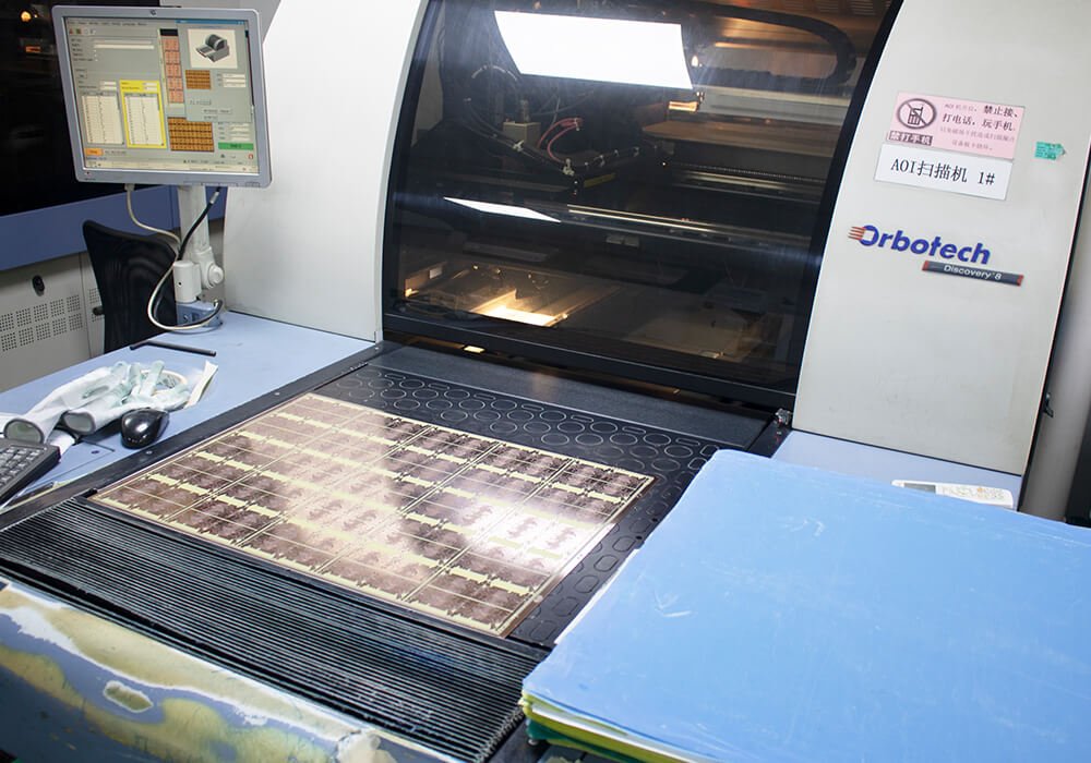
PCB AOI
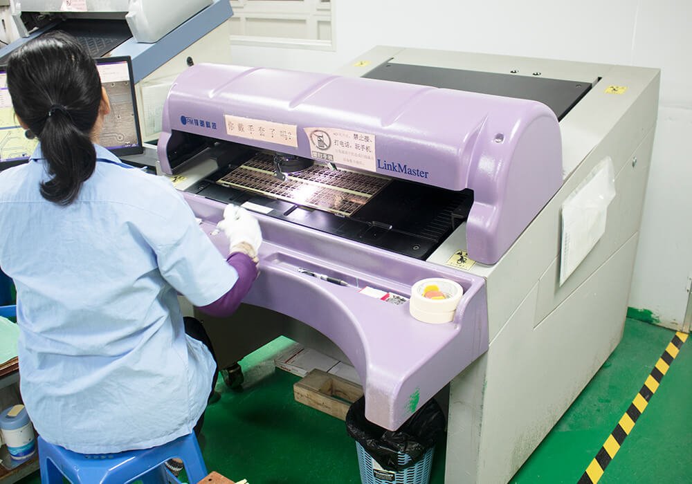
Link Master
Drill Machine
checking machine
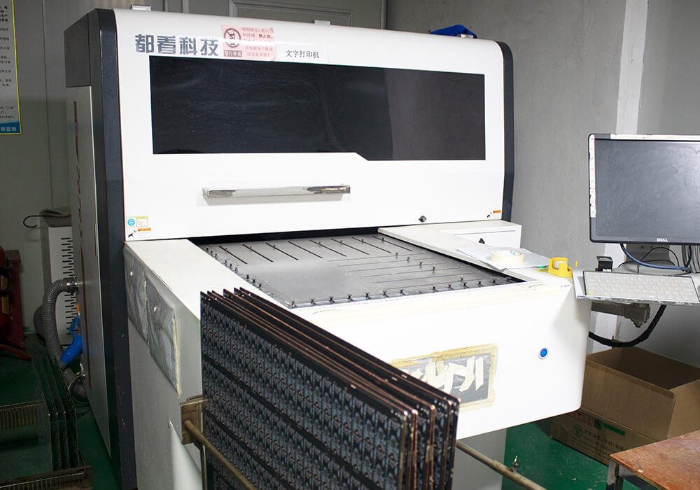
screen printing machine
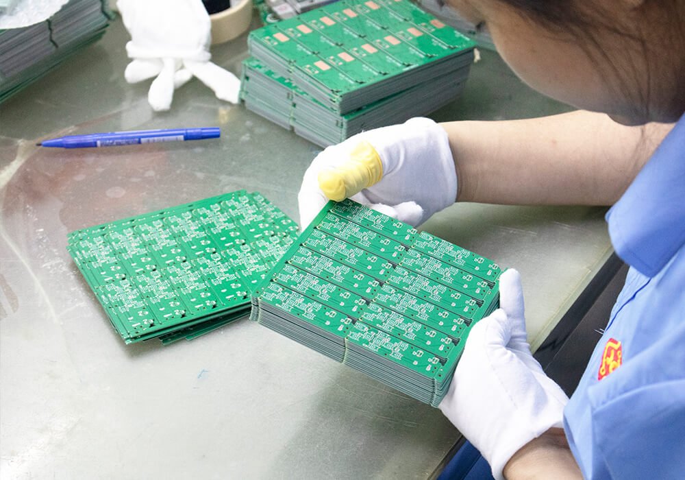
Eye Checking
PCB layout software

Engineering Review

Our engineering team will review Design for Manufacturability (DFM) and Design for Signal Integrity (DFSI) to ensure the design can be manufactured.

top 10 pcb manufacturing companies in india

Material Preparation

After design verification, the selected high-speed laminate materials and copper foils are prepared according to the specified stackup structure.

PCB layout online

LDI

Next, the circuit patterns for each inner layer are created using Laser Direct Imaging (LDI) technology. After imaging, the copper layers are chemically etched to form the final signal traces.
online pcb manufacturing

AOI

After etching, each inner layer undergoes Automated Optical Inspection (AOI) to detect potential manufacturing defects
pcb assembly parts

Lamination

Once inner layers pass inspection, they are stacked together with prepreg layers according to the PCB stackup design. The stack is then laminated under controlled heat and pressure in a multilayer lamination press.

pioneers pcb factory

Drilling and Via

After lamination, drilling processes create vias and component holes that connect different layers of the PCB.

pcb assembly smt tht

Plating

After drilling, the holes are cleaned and plated with copper to create conductive connections between layers.

pcb design online free

Back-Drilling

For high-speed designs, we will do back-drilling to remove unused portions of vias that create signal stubs.

pick and place machine for pcb assembly

Imaging and Etching

After via plating, the outer PCB layers are imaged and etched using LDI technology to create final signal routing and component pads.

fr 4 pcb design

Solder Mask and Surface Finishing

A solder mask layer is applied to protect the PCB and prevent solder bridging during assembly. After solder mask curing, a surface finish is applied to protect exposed copper pads and ensure reliable solderability.

pcb material name

Testing

Every high-speed PCB undergoes electrical testing to verify connectivity and performance.

how to set up a pcb manufacturing factory

Final Inspection

Before shipment, each PCB undergoes final quality inspection to ensure it meets all standards.

High-Speed PCB Quality Control and Testing.

In our factory, every High-Speed PCB goes through a series of quality checks to make sure it meets your design requirements before shipment. From visual inspection to electrical testing, we check the details that matter for reliable assembly and long-term performance.

PCB Chechking

Visual Inspection

Checks for scratches, copper defects, solder mask issues, and other visible problems.

AOI

Detects circuit pattern defects, such as open circuits, shorts, and missing copper.

Electrical Testing

Uses flying probe or fixture testing to check circuit continuity and isolation.

Dimensional Inspection

Verifies board thickness, hole sizes, dimensions, and tolerances.

Impedance Testing

Confirms controlled impedance meets the specified requirements.

Microsection Analysis

Examines internal layer alignment, copper thickness, plating quality, and via structure.

High-Speed PCB Applications.

High-Speed PCBs play an important role in modern electronic systems where large volumes of data must be transmitted quickly and reliably.

Aerospace

Aerospace

Aerospace and defense demand extremely reliable electronics that can perform in harsh environments while handling complex communication tasks.

  • Radar And Surveillance Systems
  • Satellite Communication Equipment
  • Flight Control Electronics
  • Military Communication Systems
  • Avionics Computing Platforms

PCB Manufacturer Automotive Electronics

Automotive Electronics

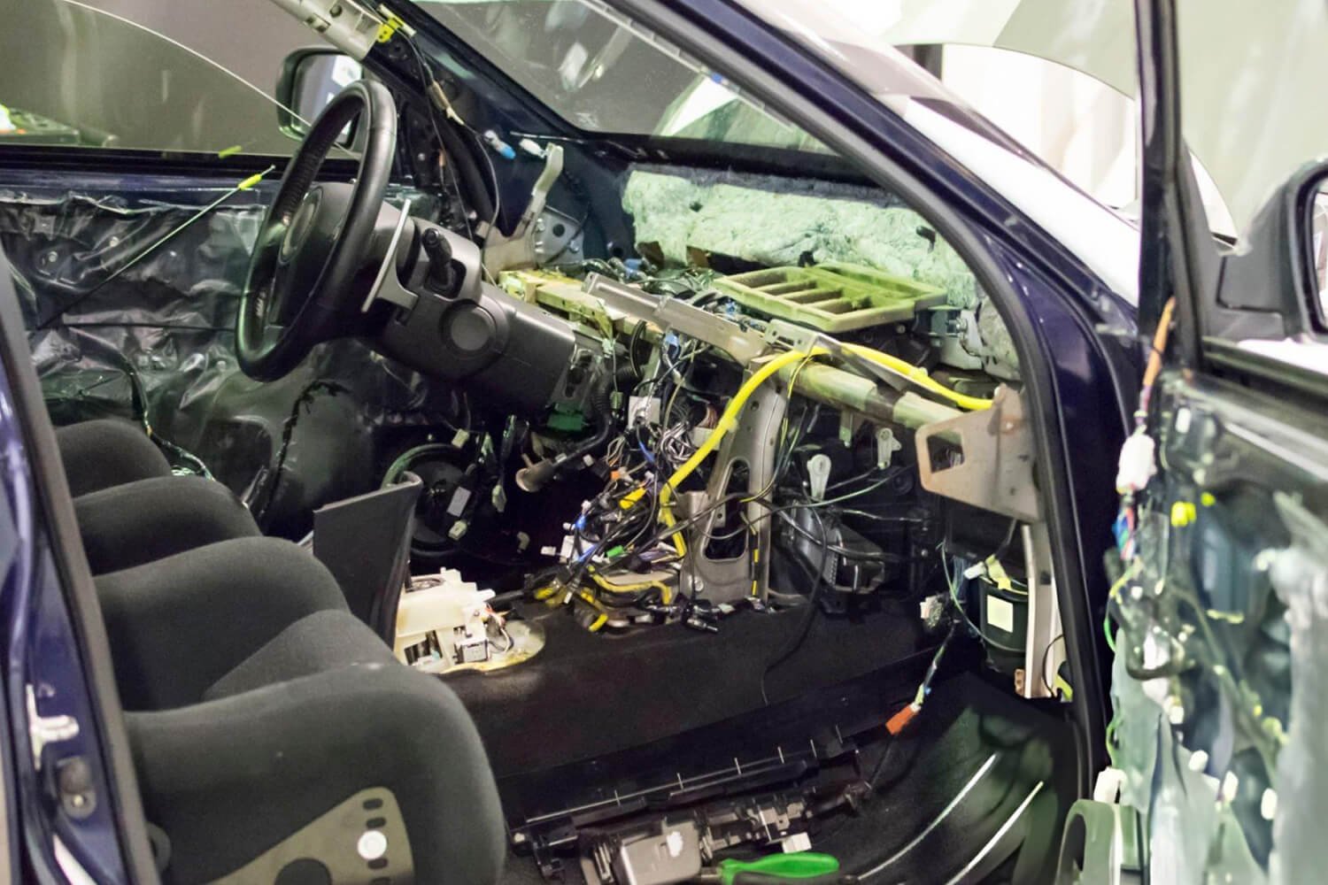
Modern vehicles are increasingly dependent on electronic systems for safety, automation, and connectivity. Many of these systems require high-speed signal processing and real-time data communication.

  • Advanced Driver Assistance Systems
  • Automotive Radar Modules
  • In-Vehicle Networking Systems
  • Autonomous Driving Control Units
  • Automotive Infotainment Platforms

PCB Manufacturer Industrial Automation

Industrial Automation

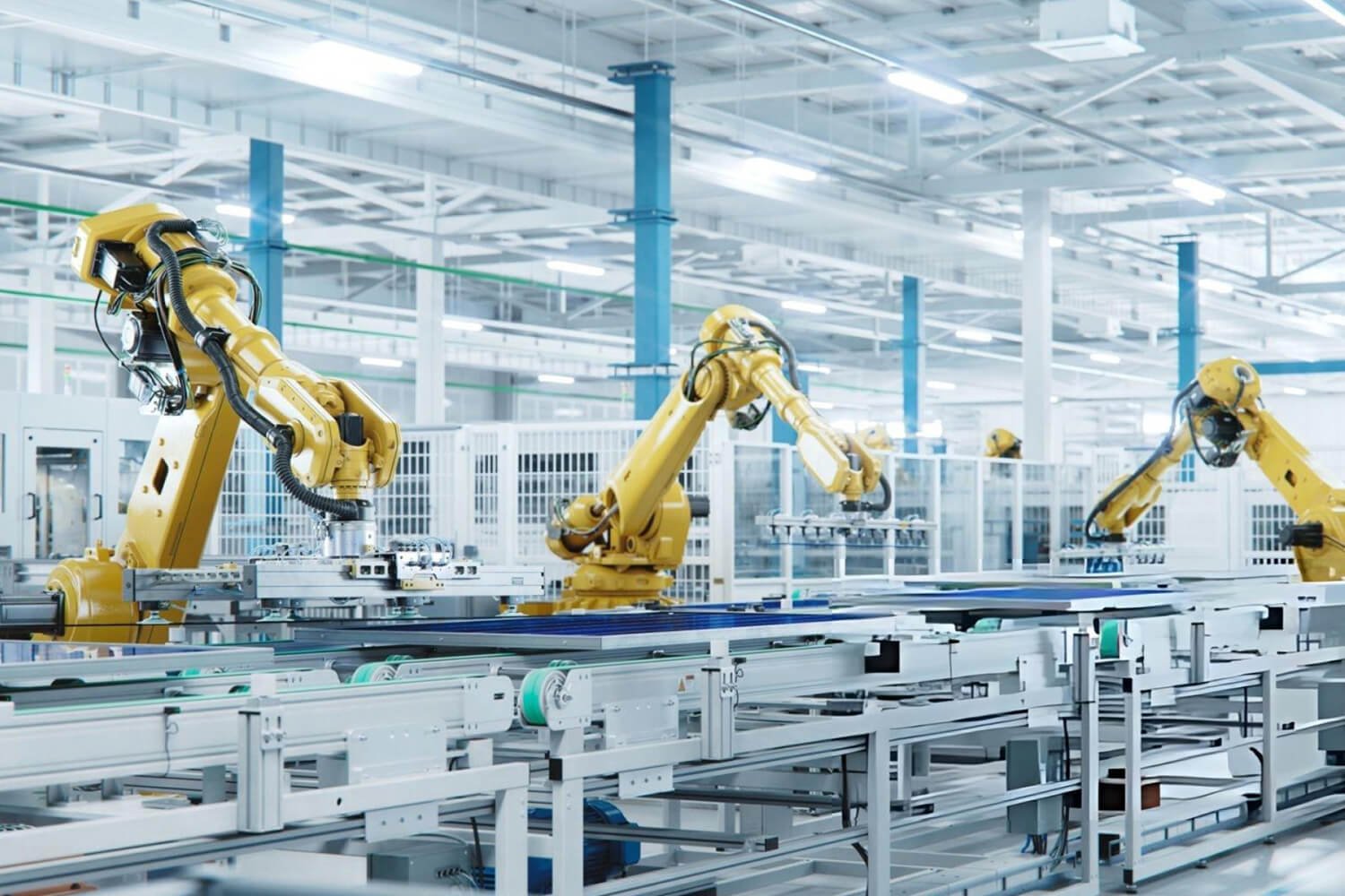
Industrial automation systems increasingly rely on high-speed data communication for precise control and real-time monitoring. High-speed PCBs enable rapid signal transmission between sensors, controllers, and processing units.

  • Robotics Control Systems
  • Industrial Networking Equipment
  • Machine Vision Systems
  • Automated Manufacturing Platforms

PCB Manufacturer Medical Devices

Medical Equipment

Medical technology often relies on high-speed electronic systems for real-time data acquisition and high-resolution imaging. High-speed PCBs help ensure accurate signal processing and stable system performance.

  • MRI Scanners
  • CT Imaging Systems
  • Ultrasound Equipment
  • Digital X-Ray Systems
  • Medical Data Processing Hardware

PCB Manufacturer Telecommunications

Telecommunication

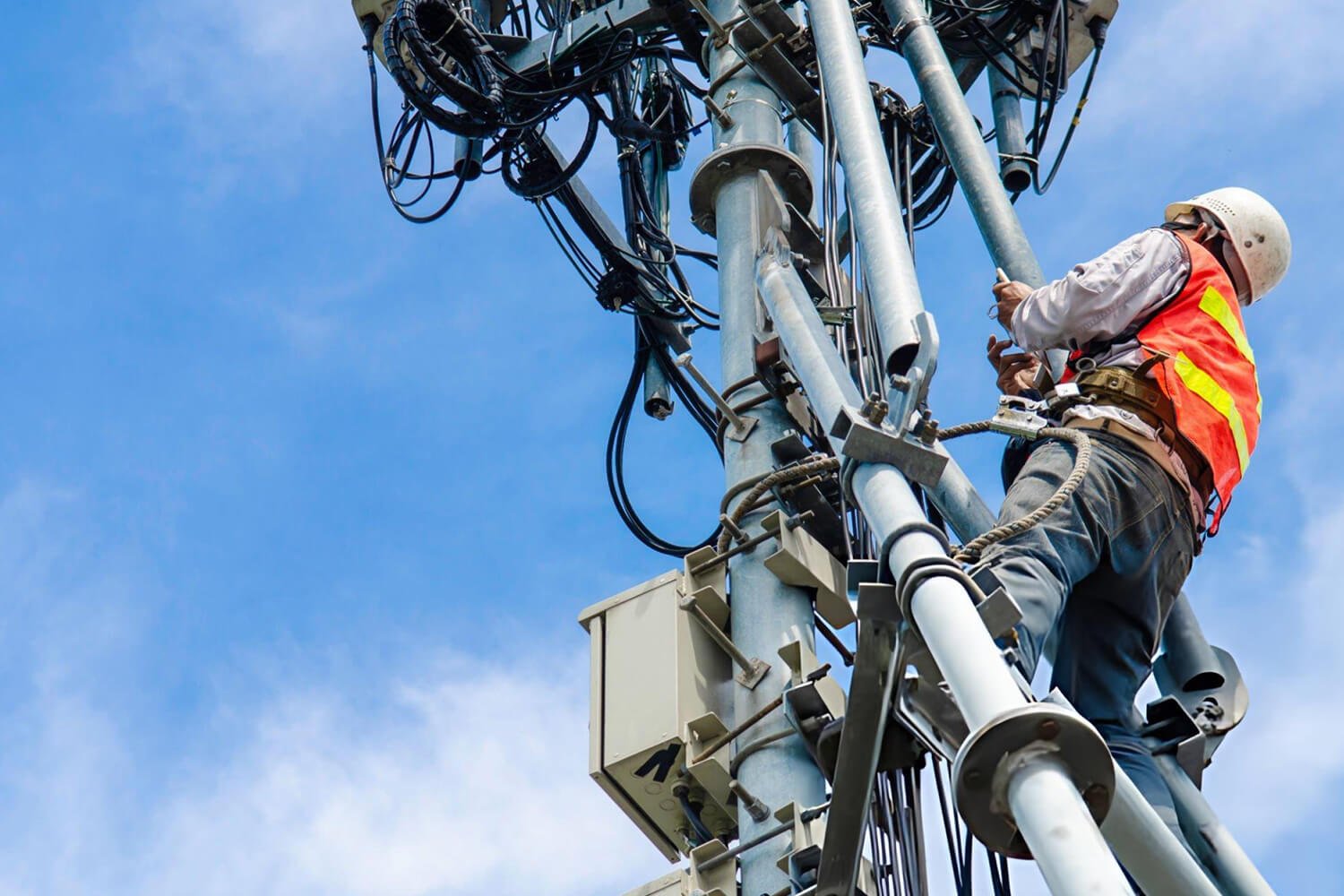
The telecommunications industry relies heavily on high-speed PCBs to handle massive volumes of data transmitted through wired and wireless networks.

  • Network Routers And Switches
  • Optical Communication Systems
  • 5G Base Stations
  • Fiber Optic Transceivers
  • High-Capacity Backplane Systems

Data Centers

Data Centers

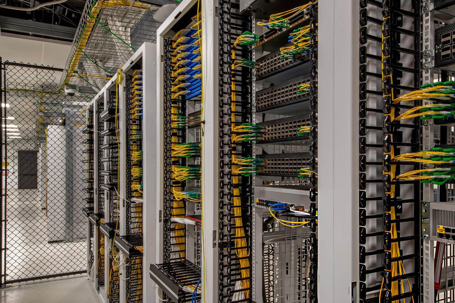
Modern data centers operate at extremely high data rates to support cloud services, artificial intelligence workloads, and global internet infrastructure. High-speed PCBs are essential for maintaining reliable communication between servers, storage systems, and networking equipment.

  • Server Motherboards
  • Network Interface Cards (Nics)
  • High-Speed Switch Fabrics
  • Storage Controllers
  • GPU Accelerator Boards

Fast Quotation.

Our professional sales and engineering teams provide fast PCB quotes and technical support. Simply send us your Gerber files, BOM, and assembly drawings, and we will respond promptly with a competitive solution.

FAQ About High-Speed PCB

1. What is a High-Speed PCB?

A High-Speed PCB (High-Speed Printed Circuit Board) is a circuit board designed to support high-frequency or high-data-rate signal transmission while maintaining signal integrity.

When signal frequencies exceed approximately 50 MHz or digital data rates reach 1 Gbps and above, the PCB begins to behave like a transmission medium rather than a simple electrical connection. At this stage, factors such as trace impedance, dielectric properties, and via structures significantly influence signal quality.

High-speed PCBs are engineered to minimize:

  • Signal reflections
  • Crosstalk
  • Electromagnetic interference (EMI)
  • Signal attenuation

These boards are commonly used in telecommunications, high-performance computing, automotive electronics, aerospace systems, and medical equipment.

A PCB typically requires high-speed design techniques when:

  • Signal frequencies exceed 50 MHz
  • Digital signals have rise times below 500 ps
  • Data rates exceed 1 Gbps

High-speed PCBs are commonly used in systems operating at:

  • 10 Gbps networking equipment
  • 25–56 Gbps SERDES links
  • 112 Gbps PAM4 communication channels

At these speeds, transmission line effects become dominant, requiring controlled impedance routing and low-loss materials.

Controlled impedance ensures that the electrical resistance of a signal trace remains consistent along its entire length.

If impedance changes occur, part of the signal may be reflected back toward the source, causing signal distortion and timing errors.

Maintaining controlled impedance helps achieve:

  • Clean signal waveforms
  • Reduced reflections
  • Better signal timing accuracy
  • Reliable high-speed data communication

Most high-speed differential signals are designed with impedance targets such as:

  • 85 Ω differential for memory interfaces
  • 90 Ω differential for USB and PCIe
  • 100 Ω differential for Ethernet and SERDES

High-speed PCBs require materials with stable electrical properties and low dielectric loss.

Common Materials Include:

  • Panasonic Megtron series laminates
  • Tachyon high-speed laminates
  • Isola I-Speed materials
  • Hybrid FR-4 and low-loss laminate combinations

These Materials Provide:

  • Low dielectric loss (Df)
  • Stable dielectric constant (Dk)
  • Improved signal transmission distance
  • Better thermal stability

Material selection depends on the target data rate, signal length, and system requirements.

Back-drilling is a PCB manufacturing technique used to remove unused portions of vias, commonly called via stubs.

Via stubs can act as small resonant structures at high frequencies, causing signal reflections and signal degradation.

Back-drilling improves high-speed signal performance by:

  • Eliminating via stub resonance
  • Reducing signal reflections
  • Improving signal integrity

This technique is commonly used in high-speed backplane PCBs and SERDES channels.

Although the terms are sometimes used interchangeably, they refer to slightly different concepts.

High-Speed PCBs

  • Focus on digital signal transmission
  • Concerned with signal integrity and timing
  • Common in computing and networking systems

High-Frequency PCBs

  • Focus on RF and microwave signals
  • Concerned with electromagnetic wave behavior
  • Common in wireless communication and radar systems

Some designs combine both technologies, especially in RF communication equipment and wireless infrastructure.

Several factors influence signal integrity in high-speed circuit boards, including:

  • Trace impedance and geometry
  • PCB material properties
  • Via structures and stubs
  • Copper surface roughness
  • Differential pair routing accuracy
  • Crosstalk between signal traces
  • Reference plane continuity

Proper PCB design and manufacturing processes help minimize these issues and maintain stable signal transmission.

Yes. Many high-speed PCBs incorporate High-Density Interconnect (HDI) technologies such as:

  • Laser microvias
  • Stacked microvias
  • Via-in-pad structures

HDI technology allows designers to integrate high-pin-count components such as processors and FPGAs while maintaining controlled impedance routing.

Yes. PCBSAIL provides custom high-speed PCB manufacturing services tailored to specific project requirements.

Our Services Include:

  • Stackup design assistance
  • Controlled impedance fabrication
  • Low-loss material processing
  • Back-drilling and microvia structures
  • High-speed PCB assembly services

Our engineering team works closely with customers to ensure that each PCB meets both electrical performance and manufacturing requirements.

Dynamic flex designs are commonly used in hinges, robotics, and camera modules.