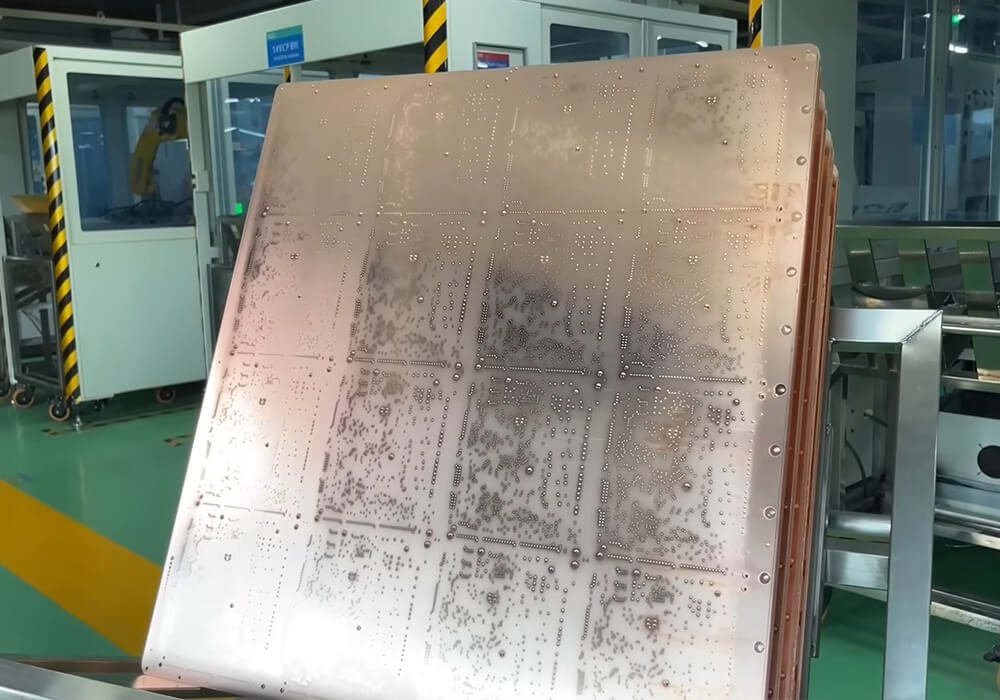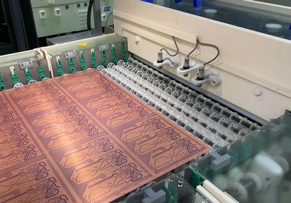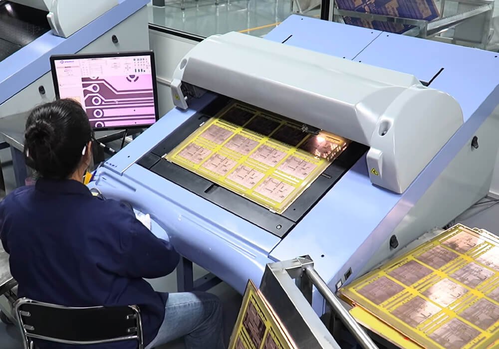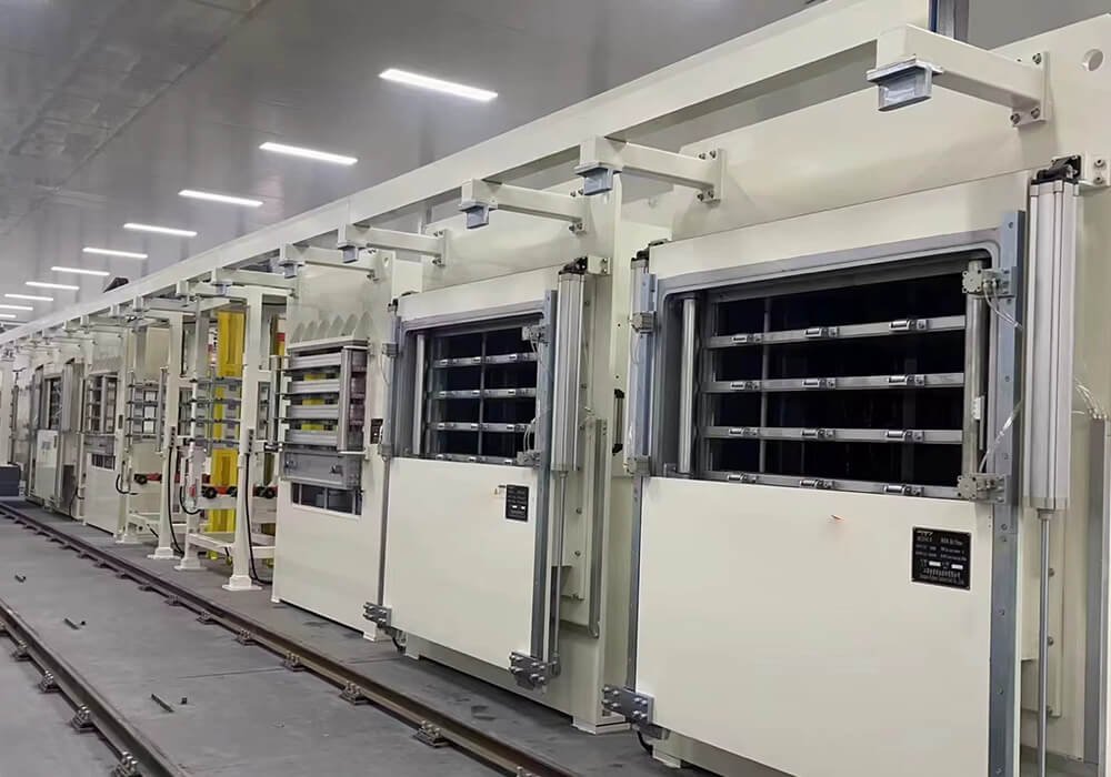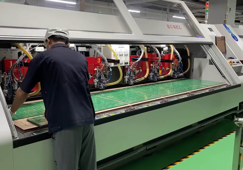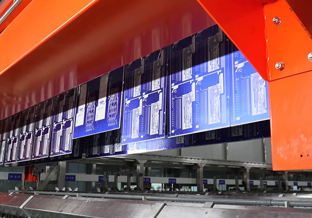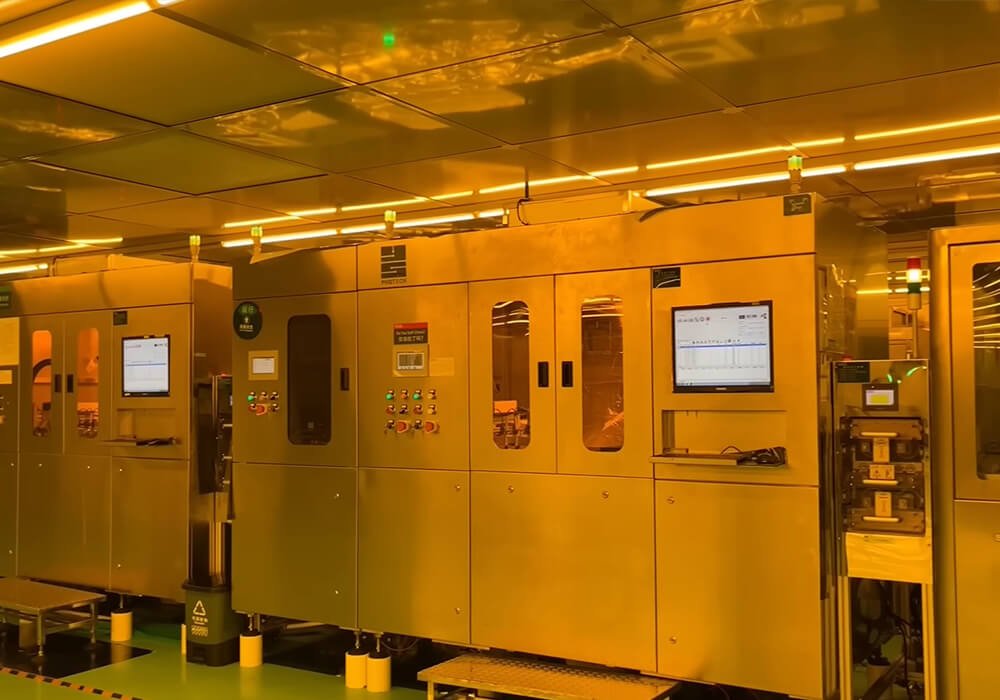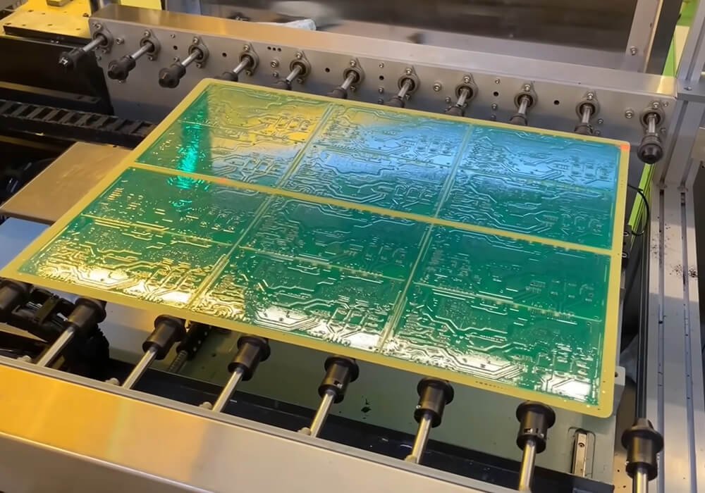
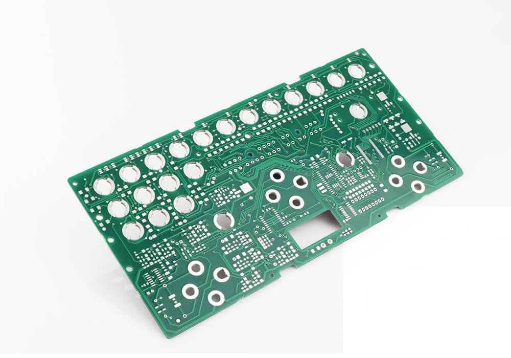
/High-Reliability Electronics/

PCB Manufacturing Services

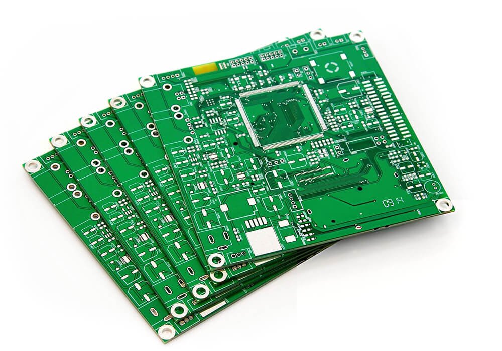
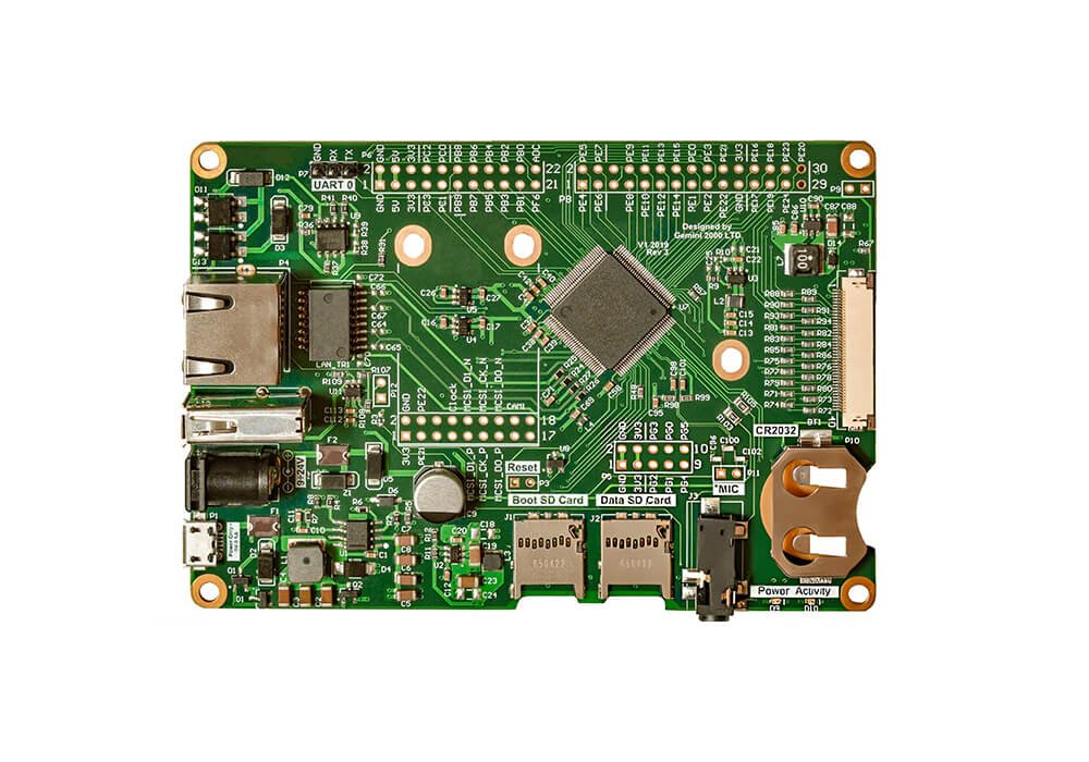
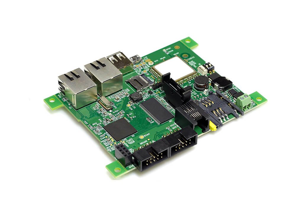
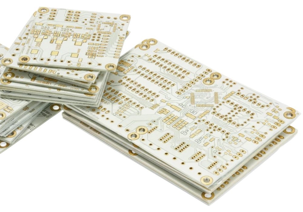
From PCB prototypes to large-scale production, PCBSAIL provides reliable PCB manufacturing services for global electronics companies, engineering teams, startups, and OEM manufacturers.

With advanced PCB fabrication capabilities, experienced engineers, and strict quality management systems, we support customers from initial PCB design verification to final production delivery.

PCB Manufacturing Trusted PCB Manufacturing Partner

Trusted PCB Manufacturing Partner .

Modern electronic products need PCBs with higher reliability, tighter tolerances, and more complex structures.

Choosing the right PCB manufacturer directly affects:

  • Product Reliability
  • Manufacturing Cost
  • Time-To-Market
  • Long-Term Supply Stability
  • Compliance With Industry Standards

We provided complete PCB manufacturing solutions with flexible production capability, supporting customers throughout the entire product lifecycle.

Feature PCB.

Modern electronic products require different PCB structures depending on electrical performance, mechanical requirements, environmental conditions, and application scenarios.

We are capable of offering various PCBs, from standard rigid circuit boards to advanced high-performance solutions.

Cheaper Rigid PCB
Get Flex PCB
Rigid Flex PCB Manufacturer

PCB Types We Manufacture.

Multilayer PCB Near Me

Multilayer PCB

Multilayer PCBs are one of the most widely used PCB technologies for advanced electronic products. Our multilayer boards provide:

  • Higher Circuit Density
  • Better Signal Integrity
  • Improved Power Distribution
  • Reduced Product Size
  • More Design Flexibility

HDI PCB Price

HDI PCB

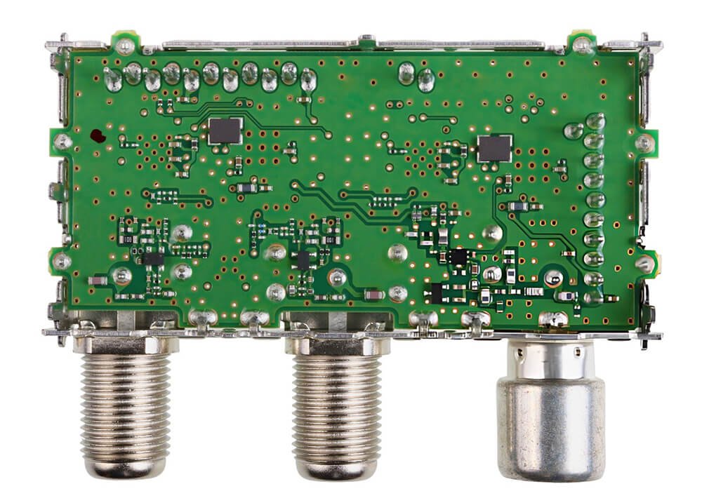
Our HDI PCB enables higher circuit density through advanced via structures. They are designed for applications that requires compact size and high performance. It can provide:
  • Higher Component Density
  • Better Signal Performance
  • Smaller Product Size

Cheaper Flex PCB Price

Flexible PCB

Flexible PCBs use flexible materials such as polyimide to create lightweight and bendable circuits. Our flexible PCB can bring you:

  • Space Saving
  • Lightweight Design
  • Improved Reliability
  • Better Mechanical Performance

Rigid Flex PCB Factory

Rigid-Flex PCB

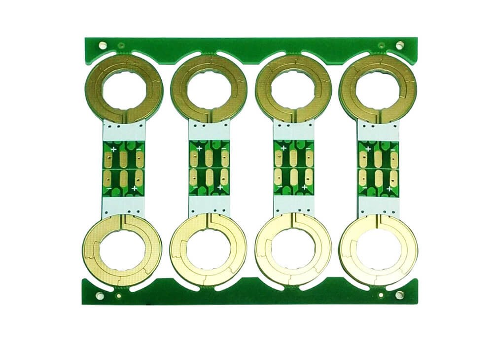
Rigid-flex PCBs combine rigid board sections with flexible circuit areas. Rigid-flex PCB eliminates additional connectors and cables. You can benefit from our Rigid-Flex PCB:

  • Reduced Assembly Complexity
  • Higher Reliability
  • Space Optimization
  • Better Mechanical Durability

Cheap High-Frequency PCB

High Frequency PCB

Our High-frequency PCBs are designed for applications requiring stable electrical performance at high operating frequencies. These PCBs are made of Rogers laminate or PTFE materials. It can:

  • Low Dielectric Loss
  • Stable Dielectric Constant
  • Controlled Impedance
  • Low Signal Attenuation

Best High-Speed PCB

High Speed PCB

Our high-speed PCBs can offer signal integrity in fast digital systems.

When designing high-speed PCBs, you need to carefully control of:

  • Impedance
  • Trace Geometry
  • Layer Stack-Up
  • Material Selection
  • Return Paths

Cheaper High Tg PCB

High Tg PCB

High Tg PCB can provide improved thermal resistance compared with standard FR-4. Our high Tg materials provide:

  • Better Thermal Stability
  • Improved Dimensional Stability
  • Higher Reliability Under Heat Cycles

Best Heavy Copper PCB

Heavy Copper PCB

Heavy copper PCBs use thicker copper layers to handle higher current requirements. Compared with standard copper thickness, heavy copper PCBs provide:

  • Higher Current Carrying Capability
  • Better Heat Dissipation
  • Improved Mechanical Strength

Feature Ceramic PCB Manufacturer

Ceramic PCB

Ceramic PCBs are designed for extreme thermal and electrical performance. It can offer: Excellent Thermal Conductivity High Temperature Resistance Low Thermal Expansion Superior Reliability

Item

Prototype 

Bulk Order

PCB Material

FR4,Ceramic ,Aluminum base, Copper base,Others

FR4,Ceramic, Aluminum Base, Copper Base, Others

PCB Type

Single-sided/Multi-layer PCB/HDI/High Frequency PCB/High Speed PCB/Heavy Copper PCB

Number of Layers

2-64

2-32

PCB Thinckess

0.2-3.5mm

PCB SIZE(Max.)

1050*610MM

800*600MM

Copper Foil Thickness

1/4-12OZ

1/3-6OZ

Mechenical Hole

5mil(0.127mm)

6mil(0.15mm)

Laser Hole

3mil(0.076mm)

4mil(0.1mm)

Line Width/Spacer

Inner Layer1.8/1.8mil, top layer2/2mil

Inner Layer2/2mil, top layer2.5/2.5mil

Outline Tolerance

±2mil(0.05mm)

±3mil(0.076mm)

BAG Solder Pad

7mil(0.18mm)

8mil(0.2mm)

Through Hole Aspect Ratio

20:1

12:1

Blind Hole Aspect Ratio

1:1

1:1.2

Impedance Tolerance

5%

8%

Distance From Hole To Inner Layer Circuit

5mil(0.127mm)

6mil(0.15mm)

Inter-layer Alignment

2mil(0.05mm)

3mil(0.076mm)

Special Process

Center Hole, Step Hole, Countersunk Hole, Crimping Hole, Back Drilling,Two Steps, Buried Capacitor And Buried Resistor

Center Hole, Step Hole, Countersunk Hole, Crimping Hole, Back Drilling

Surface Treatment

HASL, ENIG, Immersion Tin, OSP, Immersion Silver,Electroplating Hard Gold/Soft Gold, Gold Finger,

Copper Thickness of Outer Layer(Max.)

6OZ

Soldermask Bridge Width

0.01mm

Aperture Ratio

10:1

Soldermask Color

White, Green, Yellow, Red, Black,Blue,Pink,Purple,Others

Gold Finger Hypotenuse Angle

20° 

Gold Finger Bevel Depth

0.1mm

V-cut

Normal v-cut, Jumping v-cut

Normal v-cut, Jumping v-cut

Panel Size(Max.)

20*20inch

20*20inch

Panel Size(Min.)

100*120mm

100*120mm

HDI PCB-Structure

Any Layer(10L)

HDI PCB-Width/Space (Outer Layer)

2.5mil/2.5mil

Aspect Ratio(Blind Hole)

1:1

Solder Ring(Min.)

3mil

BGA Pad Diameter(Min.)

8mil

PCB Thickness(Min.) 

0.15mm(2L)

Finished Board Size(Min.)

10mm

Impedance Tolerance

±10%, 50Ωor less:±5Ω

Bending Tolerance

0.50%

0.70%

Tin Spray Hole Diameter(Min.)

0.4mm

0.5mm

Circuit Spray Tin(Min Spacer)

10mil

12mil

Acceptance Criteria

IPC2,IPC3

Item

Prototype 

Bulk Order

Product Type

FPC, Rigid-Flex PCB

Number of Layers

1-48L Flexible PCB,2-48L Rigid-Flex PCB

1-32L Flexible PCB,2-32L Rigid-Flex PCB

Finished FPC Size

250*4000mm

PCB Thickness

FPC: 0.06-0.4mm,Rigid-Flex: 0.25-6.0mm

Line Width/Spacer

0.045mm/0.045mm

Aspect Ratio (Finish Hole)

16:1

10:1

Material

PI/PET/ED/RA

Finished Thickness Tolerance

±0.03mm

Copper Foil Thickness

12μm,18μm,36μm,70μm

Insulation Layer Thickness

12.5μm,25μm,50μm

Drilling Hole(Min.)

Mechanical Drilling: 0.15mm, Laser Drilling: 0.1mm

Vias Tolerance

±0.05mm

Reinforce

FR4/PI/PET/SUS/PSA

Surface Treatment

HASL, ENIG, Immersion Tin, OSP, Immersion Silver,Electroplating Hard Gold/Soft Gold, Gold Finger,

HeavyCopper(Max. Copper Thickness) Rigid-Flex

2Oz

Finished Impedance Control

50-120Ω

Certification

UL,E506860;Others

Environmental Certification

ROHS;SGS;REACH 168;ISO14000;Others

FPC ROUTING TOLERANCE(MM)

±0.05mm

±0.1mm

Soldermask

Green,Red, Yellow,Blue,White,Black,Purple,Pink,Others

Silk Screen

White,Black,Yellow

HDI

2+C+2

Structure   

Book, Air- gap, Fly- tail, Unsymmetrical, Semi- flex

Acceptance Criteria

Factory standard;GB;IPC-650;IPC-6012;IPC-6013 II;IPC-6013 III;military standard

"Ready To Start Building Your PCB?"

Standards for PCB.

Our PCBs complies with strict manufacturing standards and quality management systems.

PCB Certificate

IEC 61851

IEC 61851 defines requirements for conductive charging systems

PCB Certificate

ISO Standard

A controlled manufacturing environment ensures consistent quality.

PCB Certificate

IPC standard

Our PCB follows IPC standard.

PCB Certificate

RoHS

Our PCB manufacturing processes meet RoHS compliance requirements.

PCB Materials

PCB material is one of the most important decisions during PCB manufacturing. It defines the PCB’s Electrical Performance, Thermal Performance, Mechanical Reliability, and Manufacturing Cost. We will purchase the high-quality material from verified supplier to ensure PCB performance.


PCB Manufacturing PCB Materials

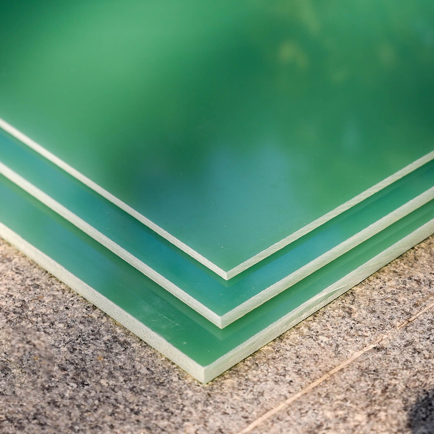
FR-4 is the most widely used PCB substrate material worldwide. It is a fiberglass-reinforced epoxy laminate.

It can offer

  • Cost Effective: FR-4 provides excellent performance at a competitive cost.
  • Easy Manufacturing: Most PCB manufacturers have extensive experience processing FR-4 materials.
  • Good Mechanical Strength: The fiberglass structure provides excellent rigidity and durability.
  • Wide Availability: FR-4 materials are available in many thicknesses and grades.

High Tg FR-4 is an enhanced version of traditional FR-4 designed for improved thermal reliability. It maintains mechanical stability at higher operating temperatures.

High Tg FR-4 Provides:

  • Better Thermal Resistance
  • Improved Dimensional Stability
  • Reduced Thermal Expansion
  • Higher Reliability

Rogers are widely used for high-frequency and microwave applications.

Compared with standard FR-4, Rogers materials provide:

  • More Stable Dielectric Properties
  • Lower Signal Loss
  • Better Frequency Performance

Popular Rogers Materials Include:

  • Rogers RO4003C
  • Rogers RO4350B
  • Rogers RT/duroid series

PTFE (Polytetrafluoroethylene) is a high-performance dielectric material used in demanding RF applications. It provides extremely low electrical loss.

PTFE offers:

  • Very Low Dielectric Loss
  • Excellent High-Frequency Performance
  • Stable Electrical Characteristics

Metal Core PCBs use a metal base layer to improve thermal management.

Common Metal Cores Include:

  • Aluminum
  • Copper

Metal Core PCB provides:

  • Excellent Heat Dissipation
  • Better Mechanical Strength
  • Improved Thermal Reliability

Ceramic are advanced materials designed for extreme thermal and electrical applications.

Common Ceramic Substrates Include:

  • Aluminum Oxide (Al₂O₃)
  • Aluminum Nitride (AlN)
  • Silicon Carbide (SiC)

Ceramic PCBs provide:

  • Excellent Thermal Conductivity
  • High Temperature Resistance
  • Low Thermal Expansion
  • Long-Term Reliability

PCB Manufacturing Process

Our PCB manufacturing process goes through multiple precision manufacturing stages to transform design files into finished circuit boards

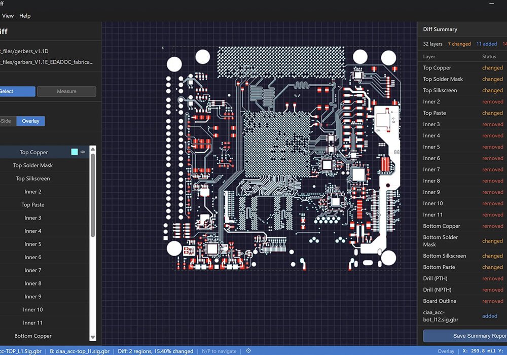
PCB Manufacturing 1.Engineering Review

Before manufacturing begins, our PCB engineers analyze the customer’s design files to ensure the PCB can be produced reliably.

We will review:

  • Gerber Files
  • Excellon Drill Files
  • PCB Layer Stack-Up Information
  • Fabrication Drawings
  • Netlist Files
  • Bill Of Materials (For PCBA Projects)
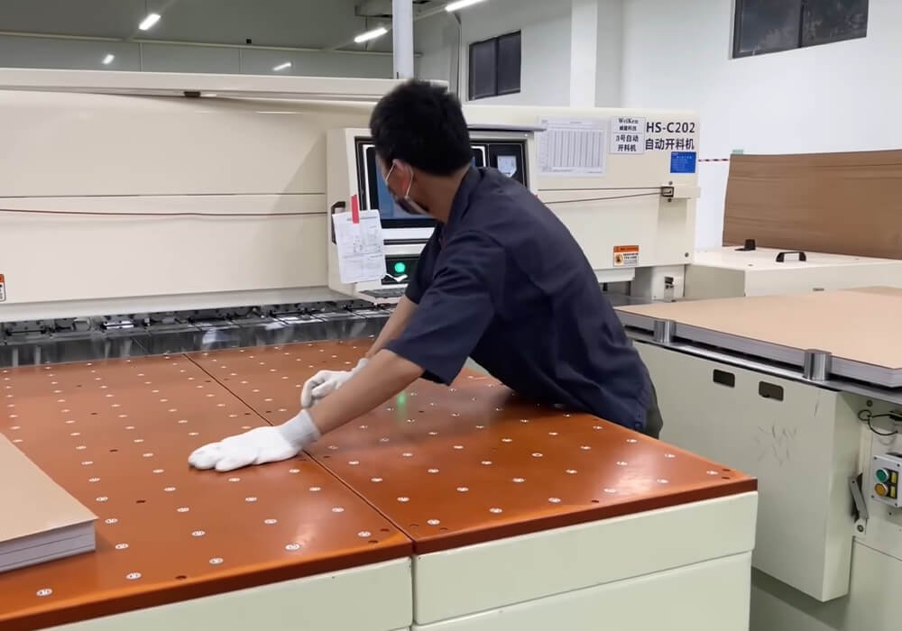
PCB Manufacturing 2.Material Preparation

After design approval, PCB production begins with material preparation. After confirming the PCB material, we will process these materials.

Typical PCBs are composed of :

  • Copper Foil: Provides electrical conductivity.
  • Dielectric Layer: Provides insulation between copper layers.
  • Core Material: Provides mechanical strength.
  • Prepreg: A bonding material used during lamination.
PCB Manufacturing 3.Inner Layer Imaging Copper Surface Cleaning

Copper surfaces are cleaned to remove:

  • Oxidation
  • Dust
  • Contamination

A clean surface ensures proper photoresist adhesion.

PCB Manufacturing 4.Inner Layer Imaging Circuit Pattern Exposure
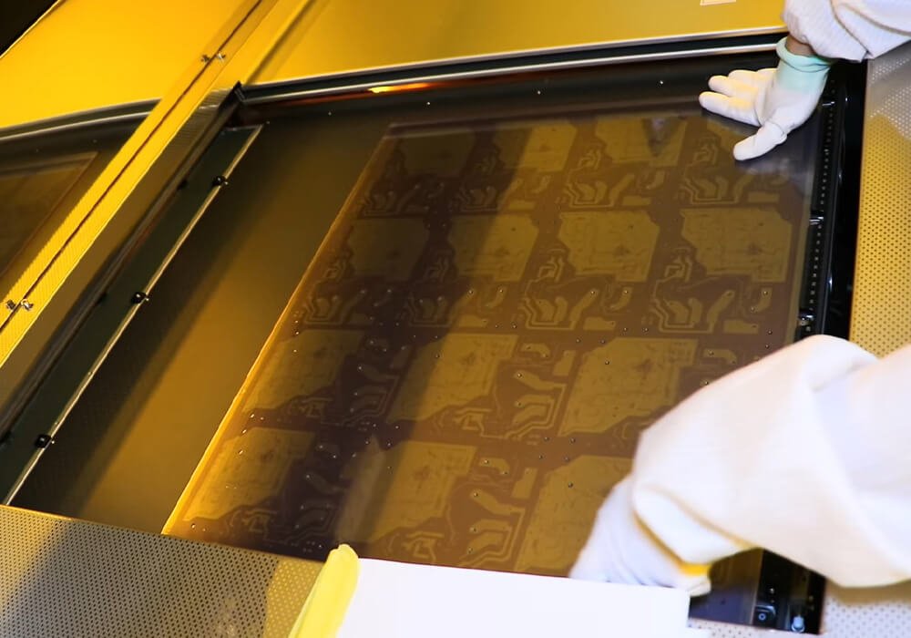
The PCB artwork is transferred onto the photoresist using:

  • Laser Direct Imaging (LDI)
  • Photolithography systems

The exposed areas define the circuit pattern.

PCB Manufacturing 5.Inner Layer Etching

After imaging, unwanted copper is removed through chemical etching. The process creates the actual circuit pattern.

Etching Process

  • Protected copper remains
  • Exposed copper is removed

The result is a precise inner-layer circuit.

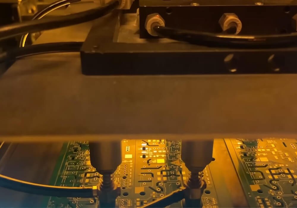
PCB Manufacturing 6.Inner Layer AOI

After etching, inner layers undergo Automated Optical Inspection. AOI systems compare the manufactured PCB layer with the original design database.

AOI Detects:

  • Missing Traces
  • Extra Copper
  • Short Circuits
  • Broken Circuits
  • Pattern Defects
  • Alignment Errors

AOI inspection is critical because inner-layer defects become impossible to repair after lamination.

PCB Manufacturing 7.Layer Lamination

Multilayer PCB manufacturing requires bonding multiple layers into one solid structure.

  • Lamination Process Steps 1. Layer Alignment

All PCB layers are precisely aligned using optical targets. High accuracy is required because even small alignment errors can affect via connections and signal performance.

  • Lamination Process Steps 2. Heat and Pressure Application

The stacked PCB layers are placed into a lamination press to create a permanent bond.

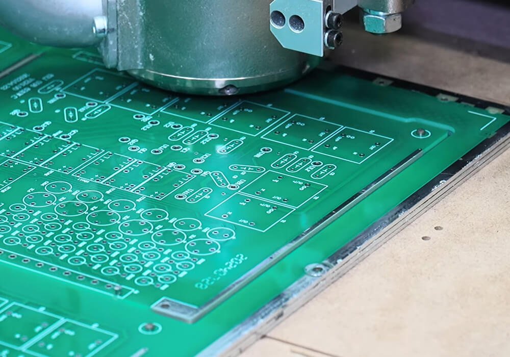
PCB Manufacturing 8.CNC Drilling Process

After lamination, holes are drilled into the PCB.

PCB drilling creates:

  • Through holes
  • Via holes
  • Component mounting holes
PCB Manufacturing 9.Copper Plating Process

After drilling, hole walls are not conductive. Copper plating creates electrical connections between PCB layers.

  • Plating Steps 1. Chemical Copper Deposition

A thin copper layer is deposited onto hole walls and PCB surfaces.

  • Plating Steps 2.Electrolytic Copper Plating

Additional copper thickness is added to improve current carrying capability and mechanical reliability.

PCB Manufacturing 10. Outer Layer Imaging and Etching

The outer layer imaging and etching is one of the most critical stages in PCB manufacturing. It creates the external copper circuit patterns that connect electronic components, connectors, and other electrical elements on the finished printed circuit board.

It Includes:

  • Photoresist Coating
  • Circuit Imaging
  • Copper Plating
  • Etching
  • Inspection
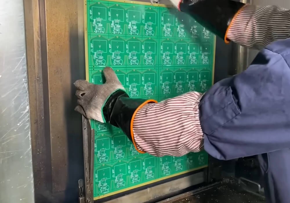
PCB Manufacturing 11.Solder Mask

The solder mask is a protective coating applied over the PCB surface. It is commonly recognized as the green layer covering most PCBs.

Solder mask provides:

  • Prevents copper oxidation and environmental damage.
  • Prevents accidental short circuits.
  • Prevents solder bridges during assembly.

Common Solder Mask Colors

  • Green
  • Black
  • Blue
  • Red
  • White
  • Yellow

The color choice usually depends on customer preference.


PCB Manufacturing 12.Surface Finish

The exposed copper pads require protection before component assembly. Surface finish improves solderability, corrosion resistance, and storage life.

Common PCB Surface Finishes

PCB Manufacturing 13.PCB Cutting and Profiling

After surface finishing, individual PCBs are separated from production panels.

Methods Include:

  • CNC routing
  • V-scoring
  • Laser cutting
PCB Manufacturing 14.Electrical Testing

Before shipment, finished PCBs undergo flying probe testing.

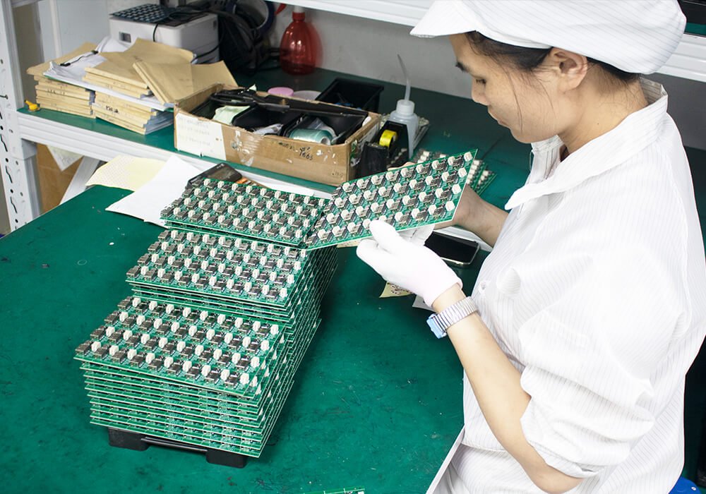
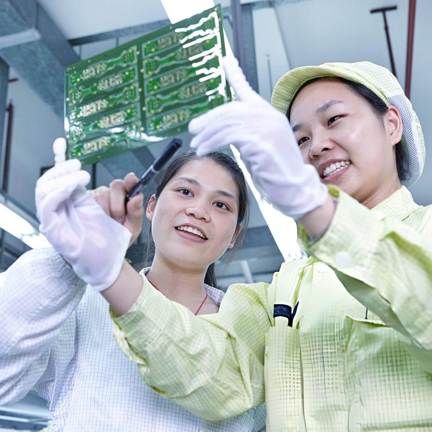
PCB Manufacturing 15.Final PCB Inspection

The final quality inspection ensures that every PCB meets customer specifications.

Our inspection teams verify:

  • PCB Appearance
  • Hole Quality
  • Surface Finish
  • Marking Accuracy
  • Quantity
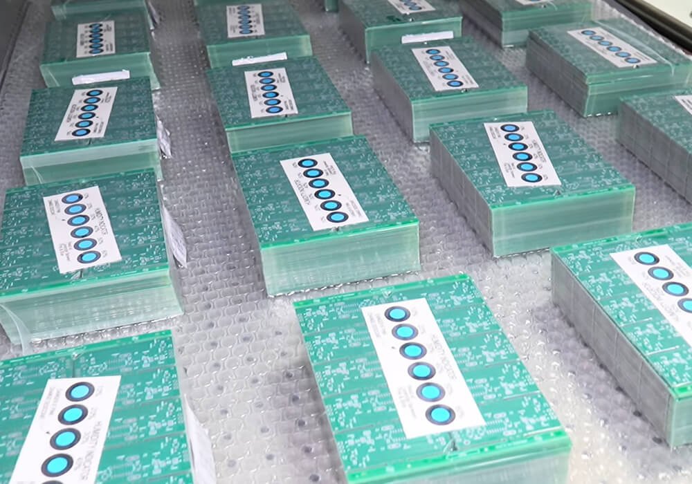
PCB Manufacturing 16.Packaging

After passing inspection, PCBs are packaged carefully.

We will pack it with:

  • Vacuum sealing
  • Moisture barrier bags
  • Protective packaging materials

PCBs are then shipped to customers worldwide.

Why Choose Us?

We provided the complete PCB manufacturing and PCB assembly solutions for global customers, supporting projects from early prototypes to full-scale production.

With advanced manufacturing capabilities, experienced engineers, strict quality management systems, and comprehensive PCB technologies, we help you develop reliable electronic products with faster and more efficient.

PTH
copper immersion
Degumming Residue
sink gold
PCB Drill Machine
PcB Manufacturing Machine
Etching
Imaging room
PCB Test Machine
PCB Checking
PCB Checking Machine
PCB Chechking
PCB AOI
Link Master
Drill Machine
checking machine
screen printing machine
Eye Checking

Industries We Offered

We offer custom PCB manufacturing solutions for a wide range of industries, from consumer electronics to mission-critical aerospace systems.

PCB Manufacturer Industrial Automation

Automation

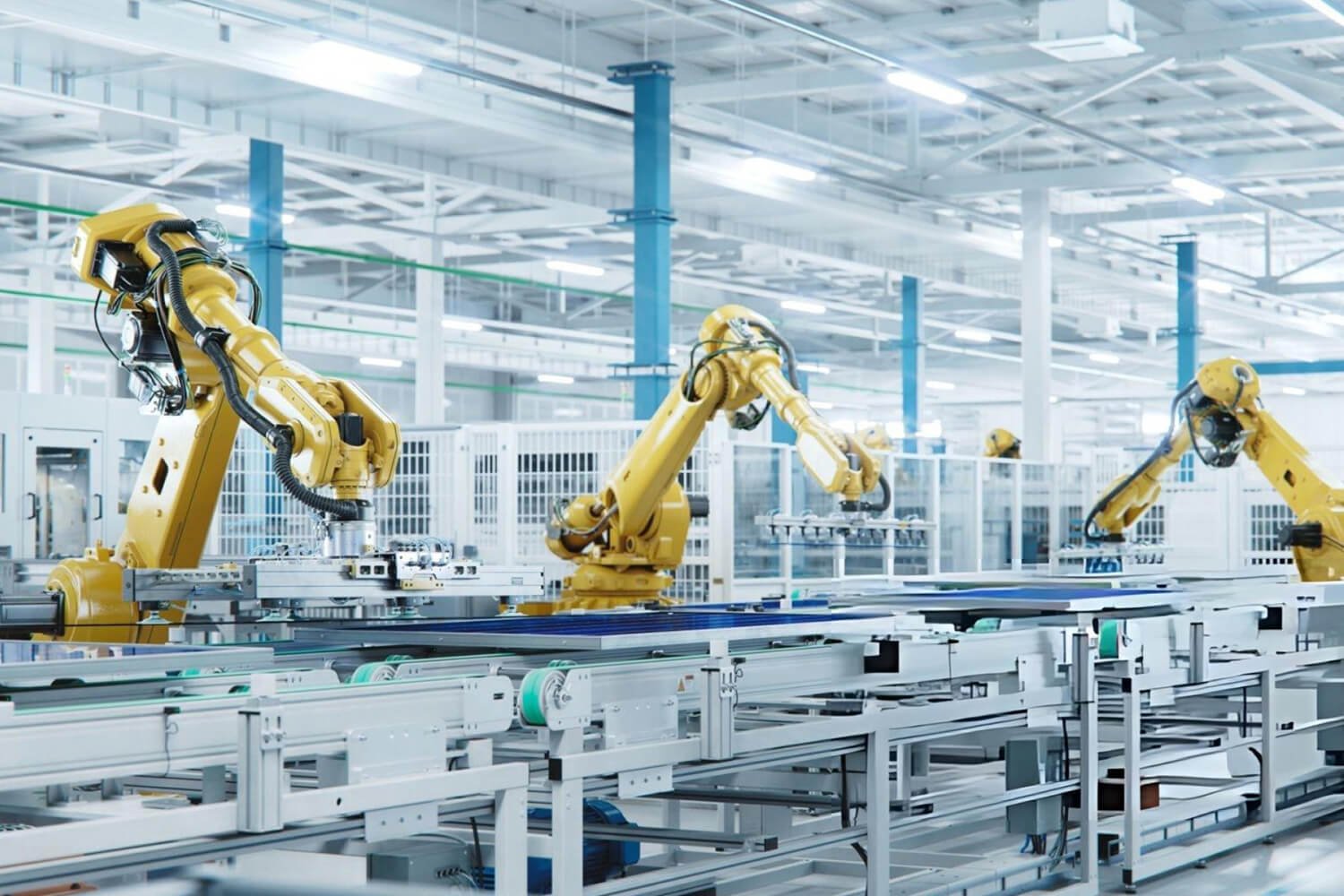
Industrial PCBs must deliver stable performance in demanding environments. We support applications that require high durability, power handling, and long operating life.

  • PLC Controllers
  • Industrial Robots
  • Servo Drives
  • Motor Controllers
  • Automation Equipment

PCB Manufacturer Automotive Electronics

Automotive Electronics

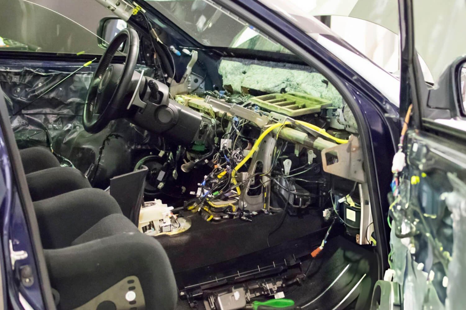
We offer automotive-grade PCBs designed to withstand harsh operating conditions, including high temperatures, vibration, and continuous operation.

  • Battery Management Systems (BMS)
  • EV Chargers
  • ADAS Modules
  • Engine Control Units (ECU)
  • Automotive Lighting Systems

PCB Manufacturer Consumer Electronics

Consumer Electronics

We manufacture high-volume, cost-effective PCBs for modern consumer products, supporting compact designs, rapid production cycles, and consistent quality.

  • Smartphones
  • Tablets
  • Laptops
  • Smart Home Devices
  • Wearable Electronics

PCB Manufacturer Power Electronics

Renewable Energy

Our PCBs support the growing renewable energy market with high-power, thermally optimized circuit boards.

PCB Manufacturer Medical Devices

Medical Electronics

Medical equipments requires strict quality management, traceability, and high manufacturing precision. Our PCB can support reliable operation for critical healthcare devices.

  • Diagnostic Equipment
  • Patient Monitoring Systems
  • Medical Imaging Devices
  • Portable Healthcare Equipment

PCB Manufacturer Telecommunications

Telecommunications

High-speed communication systems require precise impedance control and low-loss materials. Our RF and high-frequency PCBs were made from premium laminates such as Rogers and PTFE.

  • 5G Infrastructure
  • RF Modules
  • Wireless Communication Equipment
  • Satellite Communication Systems

Fast Quotation

Our professional sales and engineering teams provide fast PCB quotes and technical support. Simply send us your Gerber files, BOM, and assembly drawings, and we will respond promptly with a competitive solution.

FAQ About PCB Manufacturing

1. What Files Are Required For PCB Manufacturing?

To start PCB manufacturing, customers typically need to provide:

  • Gerber Files (RS-274X Format)
  • NC Drill Files
  • PCB Fabrication Drawing
  • Layer Stack-Up Information
  • Bill Of Materials (BOM) For PCB Assembly Projects
  • Pick-And-Place Files For SMT Assembly

We use these files to review manufacturability and prepare production data.


PCB material selection depends on electrical, thermal, mechanical, and environmental requirements.

Common Materials Include:

Material

Applications

FR-4

General electronics

High Tg FR-4

Automotive and industrial applications

Rogers

RF and high-frequency circuits

PTFE

Microwave applications

Polyimide

Flexible PCB

Aluminum Core

LED and thermal applications

Ceramic

High-power electronics

PCB manufacturing creates the bare circuit board.

The Process Includes:

  • Layer fabrication
  • Drilling
  • Copper plating
  • Etching
  • Surface finishing
  • Testing

PCB assembly adds electronic components onto the PCB.

The process includes:

We can provide both PCB fabrication and PCB assembly services.

Yes.

We support PCB prototype manufacturing for engineers and companies developing new electronic products.

Prototype services help customers:

  • Validate Designs
  • Test Functionality
  • Identify Improvements
  • Prepare For Mass Production

We supports various PCB surface finishes, including:

Surface Finish

Advantages

HASL

Cost-effective and reliable solderability

Lead-Free HASL

Environmentally compliant option

ENIG

Flat surface and excellent reliability

ENEPIG

Premium reliability and wire bonding capability

OSP

Cost-effective organic protection

Immersion Tin

Suitable for fine-pitch assembly

Immersion Silver

Good electrical performance


PCBSAIL offers multiple surface finishes:

  • ENIG
  • HASL / Lead-Free HASL
  • OSP
  • Immersion Silver
  • Immersion Tin

All finishes are RoHS compliant and compatible with lead-free assembly.

We follow internationally recognized quality standards, including:

  • IPC standards
  • ISO 9001
  • ISO 14001
  • ISO 13485
  • IATF 16949
  • UL requirements
  • RoHS compliance
  • REACH compliance

These standards ensure consistent quality and reliable PCB performance.


We uses multiple inspection and testing methods, including:

  • Automated Optical Inspection (AOI)
  • Electrical Testing
  • Flying Probe Testing
  • X-Ray Inspection
  • Impedance Testing
  • Dimensional Inspection
  • Final Visual Inspection

These processes help detect manufacturing defects before shipment.