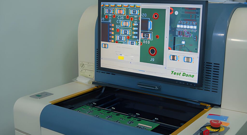
Automated optical inspection, or AOI, is a key quality-control step in modern PCB assembly. It uses cameras, controlled lighting, and software to inspect a populated circuit board against approved reference data.
AOI is especially effective at finding visible placement and soldering defects before they move into testing, enclosure assembly, or shipment.
It can quickly flag missing components, polarity errors, shifted parts, solder bridges, tombstoning, and lifted leads.
However, AOI does not prove that every solder joint is sound or every circuit works correctly. It cannot directly inspect hidden joints beneath BGA, CSP, LGA, or many QFN packages. It also cannot replace electrical or functional testing.
A practical inspection plan therefore treats AOI as one layer within a wider PCBA quality strategy.
The right combination may include solder paste inspection, X-ray inspection, ICT, flying probe testing, functional testing, and targeted manual review.
Table of Contents
1. What Does AOI Mean in PCB Assembly?
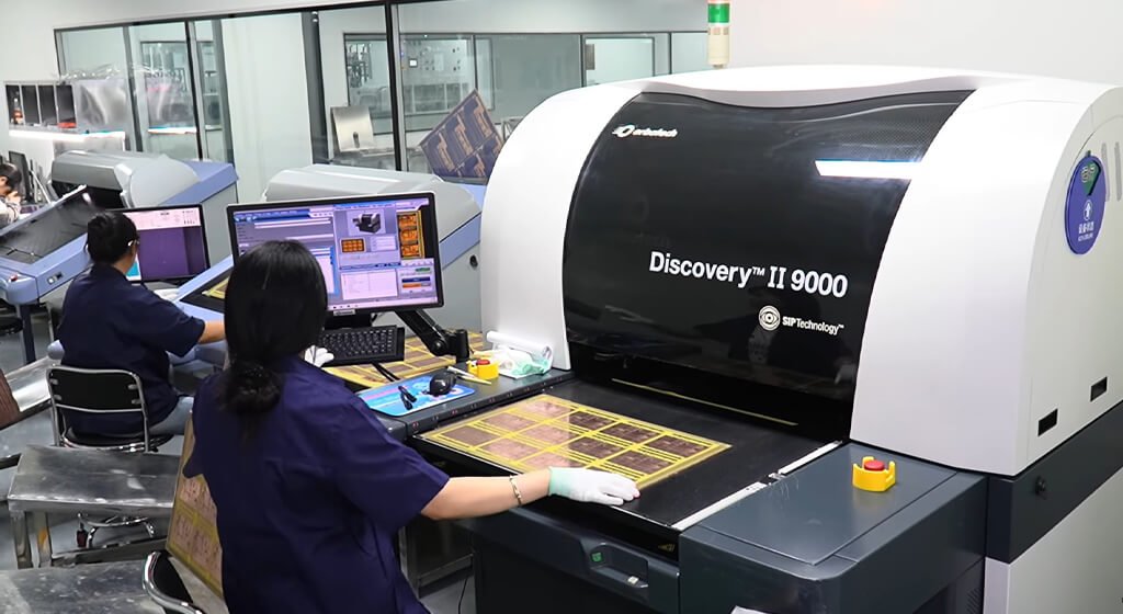
AOI in PCB assembly means automated visual inspection of a board after components have been placed, soldered, or both. The system captures images and compares visible board features with programmed inspection criteria.
Those criteria may come from CAD data, Gerber files, BOM information, pick-and-place files, component libraries, assembly drawings, or an approved golden board. The resulting program defines what the equipment should inspect and which variations require review.
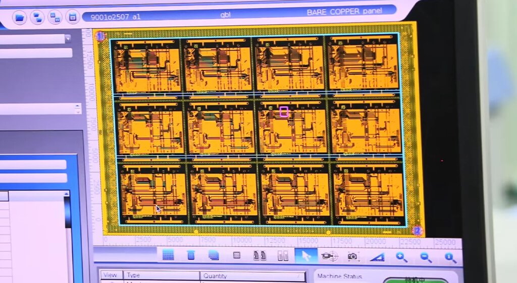
It is different from AOI used during bare PCB fabrication. Bare-board AOI focuses on copper patterns, trace geometry, opens, shorts, and other board-level features. PCBA AOI focuses on components, visible solder joints, polarity marks, placement accuracy, and assembly workmanship.
That distinction matters when discussing quality coverage with a PCB assembly supplier. A statement that a factory “uses AOI” has limited value unless it explains the inspection stage, programmed coverage, acceptance criteria, and review process.
For visual workmanship requirements, IPC-A-610J provides acceptance criteria for electronic assemblies. IPC states that it should be used alongside IPC J-STD-001J, which addresses soldered-assembly materials, methods, process requirements, and acceptance criteria.
2. Where AOI Fits in the SMT Assembly Process
AOI can appear at more than one point in an SMT line. Its value depends on when it is used and which risks the manufacturer needs to control.
A typical workflow looks like this:
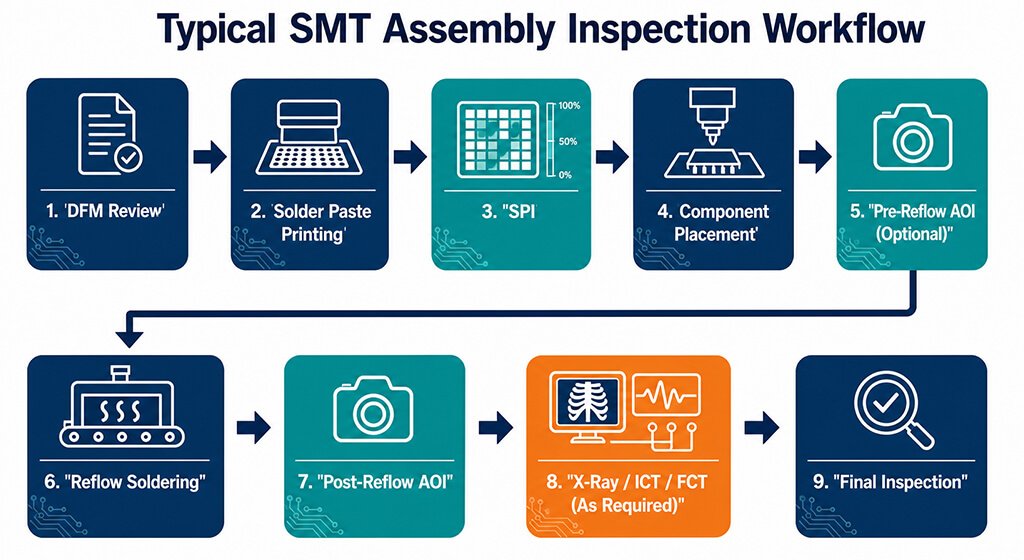
After solder paste printing, solder paste inspection, or SPI, checks whether paste was printed in the correct place and amount. SPI usually focuses on paste height, area, volume, and positional offset before components are placed.
After placement but before reflow, AOI can identify missing components, incorrect orientation, placement offsets, and obvious polarity mistakes. Catching these problems before soldering can reduce rework effort.
After reflow, AOI checks the visible condition of the completed assembly. This is the most common AOI position because it can review component placement and visible solder-joint characteristics together.
The exact production route depends on board design, package types, volume, process maturity, and customer requirements. SMT is the usual context for AOI, although mixed-technology boards may also need inspection after through-hole or selective-soldering operations.
For a broader process comparison, see PCBSAIL’s guide to SMT assembly versus through-hole assembly.
3. What Defects Can AOI Detect?
AOI is most useful for defects that are visible from the camera’s viewing angles. Good programs also use lighting and image rules that suit the component package and surface finish.
Common AOI checks include:
Defect Type | What AOI Checks | Typical Visible Condition | Recommended Follow-Up |
Missing Component | Presence against the programmed BOM and reference designator | Empty footprint or missing connector | Confirm during AOI review |
Wrong Component | Package body, color, marking, or shape where visually distinguishable | Incorrect package or visibly wrong part | Verify value and function with ICT or FCT |
Polarity Error | Orientation marks, pin-one indicators, diode bands, and connector keying | Reversed diode, IC, capacitor, or polarized connector | Review program rules before production |
Component Offset | Position relative to pads and fiducials | Part shifted beyond acceptable placement limits | Correct placement or rework before shipment |
Rotation Error | Component angle relative to the footprint | Resistor, IC, or connector rotated incorrectly | Rework and reinspect |
Tombstoning | Lead contact and component standing position after reflow | One end of a chip component lifts from its pad | Investigate paste volume, pad design, and reflow profile |
Lifted Lead | Visible lead-to-pad contact | Gull-wing lead does not sit on the pad | Rework; inspect nearby leads |
Solder Bridge | Separation between adjacent pads, leads, or balls | Excess solder connects two conductors | Remove bridge and verify electrical isolation |
Insufficient Visible Solder | Joint shape, fillet, and exposed pad coverage | Weak or incomplete visible fillet | Confirm process cause with SPI or profile review |
Excess Solder | Solder volume and spread around visible joints | Large fillet, solder splash, or unintended spread | Check stencil aperture and printing conditions |
Solder Balls And Splashes | Foreign solder around pads and components | Loose solder spheres near conductive features | Remove and review printing or reflow settings |
Damaged Component | Package body, lead shape, connector alignment, and visible cracks | Bent pin, chipped package, or damaged connector | Replace component where reliability is affected |
Bent Or Missing Leads | Lead geometry and count on visible-lead packages | Bent QFP lead or absent connector pin | Rework or replace the part |
Foreign Material | Unexpected objects or contamination on the board surface | Debris, labels, fibers, or misplaced items | Clean the assembly and identify the source |
Marking And Label Error | Barcode, label placement, polarity marking, and readable text | Incorrect label, missing label, or unreadable code | Correct before final traceability release |
AOI is fast because it applies the same rules to every board. That consistency is valuable when manual inspectors would otherwise need to review hundreds or thousands of solder joints repeatedly.
Still, speed alone does not define quality. A poorly tuned program may generate too many false calls, while an overly loose program may let defects escape.
The useful question is not whether the line has AOI equipment. The useful question is whether the inspection program reflects the actual board, package risks, and agreed acceptance criteria.
Do You Need Any Help?
4. What AOI Cannot Verify?
AOI is strongest for visible placement and solder defects. It cannot directly confirm hidden BGA joints, internal voids, electrical values, continuity, firmware, or final product behavior.
Limitation | Why AOI Cannot Confirm It | Suitable Additional Method |
Hidden BGA, CSP, Or LGA Solder Joints | The solder connections sit beneath the component body | X-ray inspection |
Internal Voids Or Cracks | These conditions are not visible from the board surface | X-ray or cross-section analysis |
Electrical Continuity And Shorts | A visually acceptable joint may still fail electrically | ICT or flying-probe test |
Component Value Or Tolerance | Similar-looking components can have different values | ICT, LCR measurement, or functional test |
Firmware And Product Behavior | AOI inspects appearance, not operational performance | Functional circuit test |
NASA’s guidance for BGA and DSBGA applications makes this point clearly. It emphasizes process control for solder attachment integrity and recommends optical and X-ray inspection together for high-reliability area-array applications. The same guidance also notes that even 2D X-ray has limits for certain damage mechanisms.
This does not mean every BGA assembly requires the same inspection scope. It means that visible inspection alone should never be treated as proof of hidden-joint integrity.
5. AOI vs. SPI vs. X-Ray vs. ICT vs. FCT
Each inspection method answers a different question. Combining them thoughtfully creates better coverage than assuming one method can do everything.
Method | Typical Stage | Best At Detecting | Cannot Replace | Common Use Case |
SPI | After solder paste printing | Paste volume, area, height, and offset | Post-reflow solder-joint review | Fine-pitch or process-sensitive SMT printing |
AOI | After placement or reflow | Visible component and soldering defects | Hidden-joint or functional verification | General SMT process control |
X-ray | After reflow | Hidden BGA/CSP/QFN solder features | Product-level functional testing | Area-array packages and inaccessible joints |
ICT / Flying Probe | After assembly | Electrical networks and selected component issues | Complete real-world product behavior | Electrical test coverage requirements |
FCT | After assembly | Functional behavior, interfaces, power-up, and performance | Visual workmanship inspection | Product-level validation |
The table should guide a conversation, not create a rigid rulebook.
For example, a simple low-volume SMT board without hidden packages may rely on post-reflow AOI plus functional testing. A dense BGA design may need AOI, X-ray, and electrical testing because each method covers different risks.
Industrial BGA X-ray study reinforces why BGA X-ray inspection remains a specialized task. Its model achieved 92.6% recall and 96.2% precision for solder-bridge detection on a limited real-production image set, while retaining human verification in the workflow. Those results are promising, but they apply only to that specific BGA scenario and model.
Do You Need Any Help?
6. 2D AOI vs. 3D AOI
2D AOI uses image contrast, shape, color, markings, and visible geometry to identify differences from programmed references. It is effective for many placement and visible soldering checks.
3D AOI adds height or shape information. This can be helpful when evaluating lifted leads, component coplanarity, tall assemblies, or solder-joint geometry that cannot be judged reliably from a top-down image alone.
Factor | 2D AOI | 3D AOI |
Primary Information | Image contrast, markings, visible shape, position | Height, shape, coplanarity, and three-dimensional geometry |
Strong Use Cases | Presence, polarity, rotation, placement offset, visible bridges | Lifted leads, component height variation, coplanarity, solder-joint shape |
Typical Advantage | Faster and suitable for many standard SMT checks | Adds geometric information where top-down images are insufficient |
Important Limitation | Limited depth information | Still cannot inspect concealed BGA or CSP solder joints |
Selection Question | Are visible placement and marking checks the main requirement? | Does the assembly need height or geometry information? |
Neither approach should be described as universally better. A 3D system may provide stronger information for certain packages, but it still cannot see through a BGA body.
The best choice depends on the board’s package mix, inspection targets, product risk, and acceptable cycle time.
7. AOI Programming, False Calls, and Engineering Review
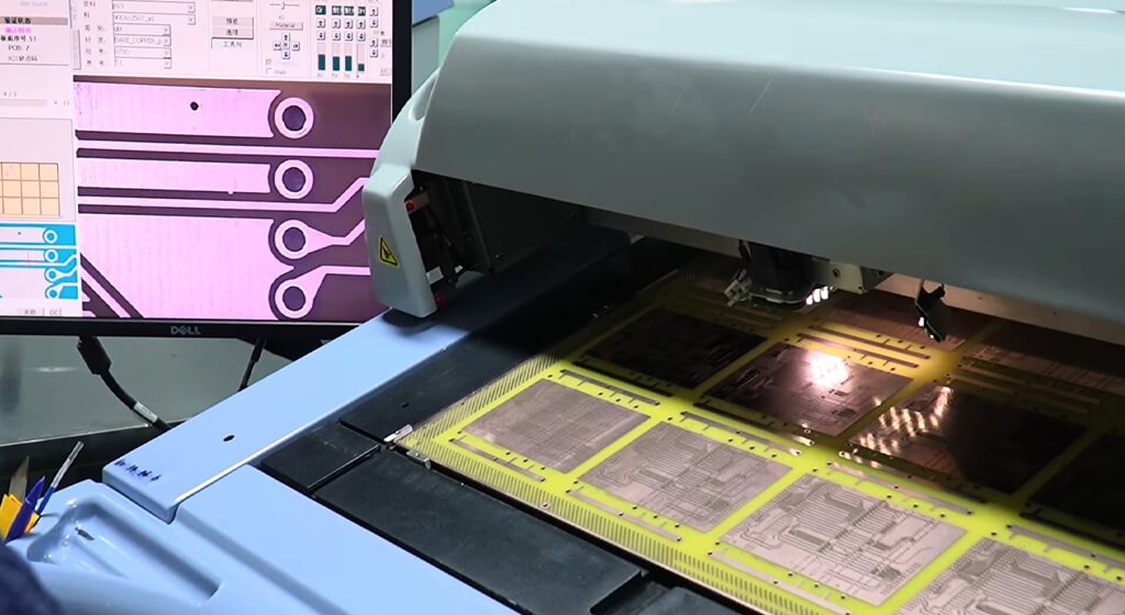
An AOI machine is only as useful as its program. Inspection performance will be affected by Lighting, component libraries, reference images, thresholds, CAD data, and golden-board approval.
A false call occurs when AOI flags a condition that is later judged acceptable. Too many false calls consume review capacity, slow production, and reduce trust in the inspection process.
A missed defect creates a different problem. If the program is too tolerant, the board may continue through testing, assembly, or shipment with a manufacturing issue that should have been detected earlier.
A 2024 data publication based on 132 days from one Siemens AG production line illustrates why this balance matters. The researchers reported that static AOI limits produced a large majority of false calls in Siemens AOI production dataset, creating substantial manual review work. They also noted distribution drift and possible human labeling error.
The lesson is practical: inspection thresholds should be reviewed using real production evidence. They should not be copied blindly from another board, package, or supplier.
The same principle applies to SPI. An IPC paste-inspection case study from Nokia and Agilent measured more than 680,000 paste bricks and subsequent solder joints in one production week. It found 46 confirmed post-reflow defects, while more than 2,000 low-paste calls did not become confirmed solder-joint defects. The authors explicitly warned that this was one case study, not a universal rule.
For buyers, this means inspection reports should show more than a simple pass or fail. A useful report may include:
Board serial number or batch identification.
- PCB revision and assembly revision.
- AOI program version and inspection stage.
- Defect images and reference images.
- Review disposition for each call.
- Rework action and verification status.
- Sampling or full-inspection scope, where applicable.
8. How to Build an Inspection Plan Around Board Risk
The most cost-effective plan is not necessarily the one with the fewest tests. It is the one that addresses the defects most likely to matter for a specific board.
Board Scenario | Suggested Inspection Focus | Why |
Simple Visible-Package SMT Prototype | Post-reflow AOI plus functional verification | Covers visible workmanship and confirms basic operation |
Fine-Pitch, High-Density SMT Board | SPI plus post-reflow AOI | Helps control paste printing and visible placement risks |
BGA, CSP, LGA, Or Hidden Thermal-Pad Design | AOI plus defined X-ray coverage | AOI cannot directly inspect concealed solder joints |
High-Volume, Stable Product | SPI, AOI, defect-trend review, and agreed electrical testing | Supports process control and consistent production decisions |
High-Reliability Or Regulated Product | Defined acceptance criteria, traceability, AOI, and risk-based supplementary tests | Requires documented coverage and controlled disposition of defects |
Testing and inspection also affect the true cost of a PCBA project. A quote should identify the required process steps rather than treating testing as an unexplained line item. PCBSAIL’s PCB Assembly Cost Guide explains the major elements that can influence assembly pricing.
9. Questions to Ask a PCB Assembly Supplier About AOI
Before approving production, ask direct questions about the inspection approach.
- At which process stage will AOI be performed?
- Is the program based on current CAD, BOM, and pick-and-place data?
- Which packages or solder joints cannot be covered by AOI?
- When is X-ray recommended, and what packages will it inspect?
- Who reviews AOI calls and confirms actual defects?
- Can the supplier provide inspection images or reports?
- How are rework and verification documented?
- Which electrical or functional tests complement visual inspection?
- What customer acceptance criteria will be used?
- Is the coverage full inspection, sampling, first-article review, or another agreed method?
These questions create a more useful discussion than asking whether the supplier has AOI equipment. They also help engineering, sourcing, and quality teams align before materials are committed.
10. AOI and Test Planning at PCBSAIL
In our factory, we can do AOI, ICT, FCT, 3D SPI, and X-ray inspection. The appropriate combination should be agreed before production according to package type, test access, product risk, and customer acceptance requirements.
Projects that require component sourcing, assembly coordination, testing, and final delivery may benefit from a turnkey PCBA service. Teams outsourcing broader manufacturing work can also review PCBSAIL’s PCB contract manufacturing services.
A complete technical package usually includes Gerber files, BOM, CPL or pick-and-place data, assembly drawings, package information, and defined test requirements. Clear input data helps engineers build inspection programs that match the actual assembly.
11. FAQ About AOI in PCB Assembly
When Is AOI Performed In An SMT Line?
AOI may be used after component placement, after reflow soldering, or both. Post-reflow AOI is common because it checks visible placement and solder-joint conditions.
Can AOI Inspect BGA Solder Joints?
AOI cannot directly inspect solder joints hidden beneath a BGA package. X-ray inspection is commonly used to evaluate hidden-joint features, although X-ray also has limitations.
Is AOI The Same As SPI?
No. SPI checks solder paste after printing and before placement. AOI checks visible components and soldering conditions after placement or reflow.
Does AOI Replace ICT Or Functional Testing?
No. AOI evaluates visual workmanship. ICT, flying probe, and functional testing address electrical connections, component behavior, and product operation.
12. Plan Inspection Before Production Begins
AOI is one of the most effective ways to catch visible PCBA defects early and consistently. Its real value comes from how it fits into a wider inspection and test strategy.
Define the package risks, acceptance criteria, data inputs, review method, and required reports before production begins. Then select AOI, SPI, X-ray, ICT, FCT, or other methods according to what the board actually needs.
For a PCBA inspection plan or quotation, provide your Gerber files, BOM, CPL file, package list, and acceptance requirements. It gives the manufacturing team the information needed to propose meaningful inspection coverage instead of a generic checklist.