
Electromagnetic interference, or EMI, is unwanted electromagnetic energy that disrupts the normal operation of an electronic product. In a PCB, it often begins with fast switching currents, noisy power converters, clocks, high-speed data lines, or poorly controlled return paths.
The best way to reduce EMI is to address it before PCB fabrication. A well-planned stackup, a continuous reference plane, small current loops, controlled impedance, and sensible component placement usually achieve more than adding shielding after a test failure.
This guide explains how EMI develops in PCB assemblies, which layout decisions matter most, and how to prepare a board for EMC testing.
It is written for engineers developing consumer electronics, industrial controls, networking hardware, medical devices, RF products, and other electronic systems.
Table of Contents
1. What Is EMI in a PCB?
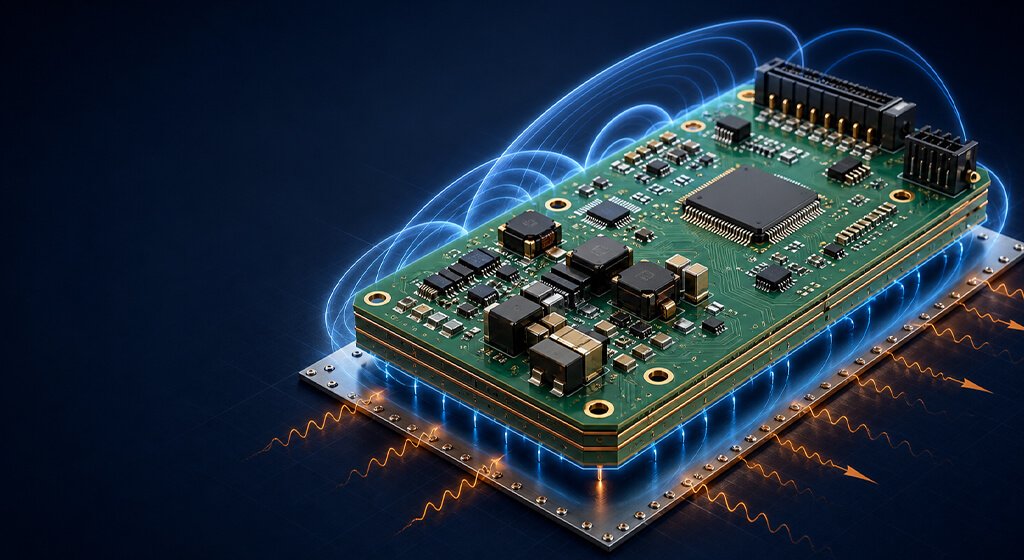
EMI is electromagnetic energy that causes unwanted effects in another circuit, cable, or electronic device. It may appear as noise on an analog signal, data errors on a digital interface, poor wireless performance, a failed compliance test, or unstable system behavior.
A PCB can both generate EMI and receive it.
For example, a DC-DC converter can generate fast current transitions. Those transitions can couple into a nearby sensor trace, escape through a cable, or radiate from a large loop on the PCB. The result may be visible noise, communication errors, or excess emissions during testing.
EMI has two common forms:
- Conducted EMI travels through power lines, signal lines, cables, and other conductive paths.
- Radiated EMI travels through electric and magnetic fields. A PCB trace, cable, connector, or enclosure opening can act as an antenna.
A useful way to analyze any EMI issue is to identify three elements: the source, the coupling path, and the victim. The source may be a switching regulator. The coupling path may be a shared ground return, parasitic capacitance, or a cable. The victim may be an RF receiver, sensitive analog input, or high-speed data lane.
Once those three elements are clear, the solution becomes much more focused.
2. EMI vs. EMC: Why the Difference Matters?
EMI and EMC are related, but they are not the same.
EMI refers to the unwanted interference itself. EMC, or electromagnetic compatibility, describes a product’s ability to operate correctly in its electromagnetic environment without causing unacceptable interference to other equipment.
In simple terms, EMI is the problem. EMC is the design and compliance objective.
A product with low radiated emissions may still have weak immunity. It may pass an emissions test but reset when a nearby radio transmitter operates. The opposite is also possible. A robust product may resist external noise but create excessive emissions of its own.
This distinction matters for products sold internationally. The European Commission explains that the EMC Directive 2014/30/EU addresses both limiting emissions and ensuring that equipment is not unduly affected by electromagnetic disturbance. European Commission guidance makes this two-way requirement clear.
Therefore, PCB EMI design should not be limited to “passing a scan.” It should support stable operation, repeatable performance, and the compliance route required by the final product market.
3. How EMI Travels Through an Electronic Product?
EMI does not need an obvious wire to reach another circuit. It can move through several coupling mechanisms, often at the same time.
Conducted coupling occurs when circuits share an electrical path. A noisy power rail may inject ripple into a sensor supply. A high-current motor return can disturb the ground reference of a microcontroller. Common impedance in a shared path is often the hidden cause.
Capacitive coupling occurs when changing voltage creates an electric field between nearby conductors. A fast clock trace near a high-impedance analog input is a classic example. The closer and longer the parallel traces are, the greater the risk.
Inductive coupling occurs when changing current creates a magnetic field. Large current loops are especially problematic. A switching regulator with a wide input loop can inject noise into nearby traces, even when the nets do not touch.
Radiated coupling occurs when PCB structures or cables behave like antennas. At higher frequencies, a discontinuous return path, a long connector cable, or an unfiltered enclosure opening can become an efficient route for emissions.
The key lesson is simple: EMI control is usually about controlling fields and current paths. It is not simply about making traces wider, adding more ground symbols, or placing a ferrite bead on every signal.
EMI Coupling Path | Typical PCB Example | Design Action |
Conducted Coupling | Switching noise shares a power or ground path with an analog circuit. | Separate noisy and sensitive power paths; use local decoupling and low-impedance returns. |
Capacitive Coupling | A fast clock runs parallel to a high-impedance sensor trace. | Increase spacing, shorten parallel runs, and place a solid reference plane nearby. |
Inductive Coupling | A large DC-DC converter loop sits close to a low-level analog input. | Minimize the high-current loop area and keep the switch node compact. |
Radiated Coupling | Common-mode current reaches an external cable or connector. | Control the connector return path; add interface filtering or common-mode suppression where justified. |
Do You Need Any Help?
4. PCB Layout Choices That Have the Largest EMI Impact
The highest-value EMI decisions happen early in layout. They are harder and more expensive to correct once the board is fabricated.
4.1. Minimize High-Current Loop Area
Every switching current needs a complete loop. The physical area enclosed by that loop matters. A larger loop creates stronger magnetic fields and increases the chance of radiated EMI.
Keep the input capacitor of a switching regulator close to the regulator’s VIN and ground pins. Keep the hot switching node compact. Place the output inductor, diode or synchronous switch, and output capacitors according to the regulator manufacturer’s recommended layout. Do not route sensitive signals under or through this noisy power stage.
The same logic applies to clock drivers, MOSFET gate-drive loops, and high-current load paths.
4.2. Place Components By Noise Region
Separate the board into functional zones. Place noisy power conversion, motor drive, RF transmission, high-speed digital logic, analog sensing, and external interfaces in deliberate regions.
This does not mean drawing arbitrary lines across the ground plane. It means reducing unnecessary interaction. Keep sensitive analog circuits away from noisy switch nodes. Place connectors near the circuits they serve. Avoid routing a quiet sensor line across a high-current power region just because it is convenient.
Good placement shortens critical routes and makes clean routing much easier.
4.3. Protect Return-Current Paths
High-frequency return current follows the path of least impedance, which is usually directly beneath its signal trace on a nearby reference plane. If the trace crosses a split, void, slot, or gap in that plane, the return current must detour.
That detour enlarges the loop. It can increase EMI, create signal-integrity problems, and inject noise into unrelated parts of the PCB.
For this reason, do not route fast signals over plane splits. If a signal must change reference planes, provide a nearby stitching via or capacitor that gives its return current a short transition path.
4.4. Avoid Unnecessary Stubs And Branches
Signal stubs can reflect energy and create resonances. They are especially harmful on high-speed digital interfaces and RF paths. Keep clock and data routes direct. Avoid long T branches unless the interface topology specifically requires them.
When a branch is unavoidable, simulate or validate it. A layout that works at low speed may behave very differently when edge rates become faster.
5. Build a Stackup That Controls Fields and Return Currents
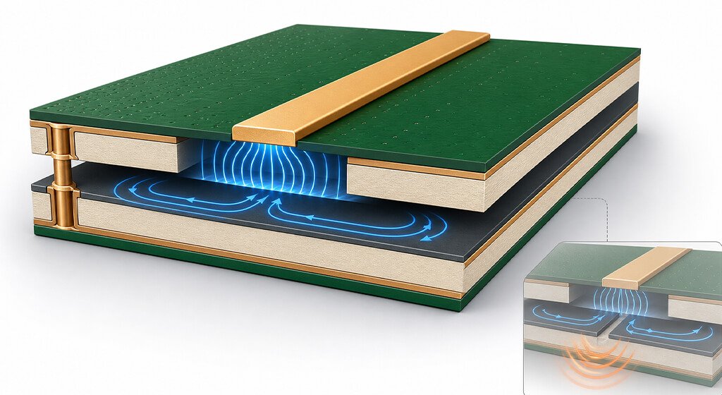
A PCB stackup is an EMI control tool, not only a manufacturing detail.
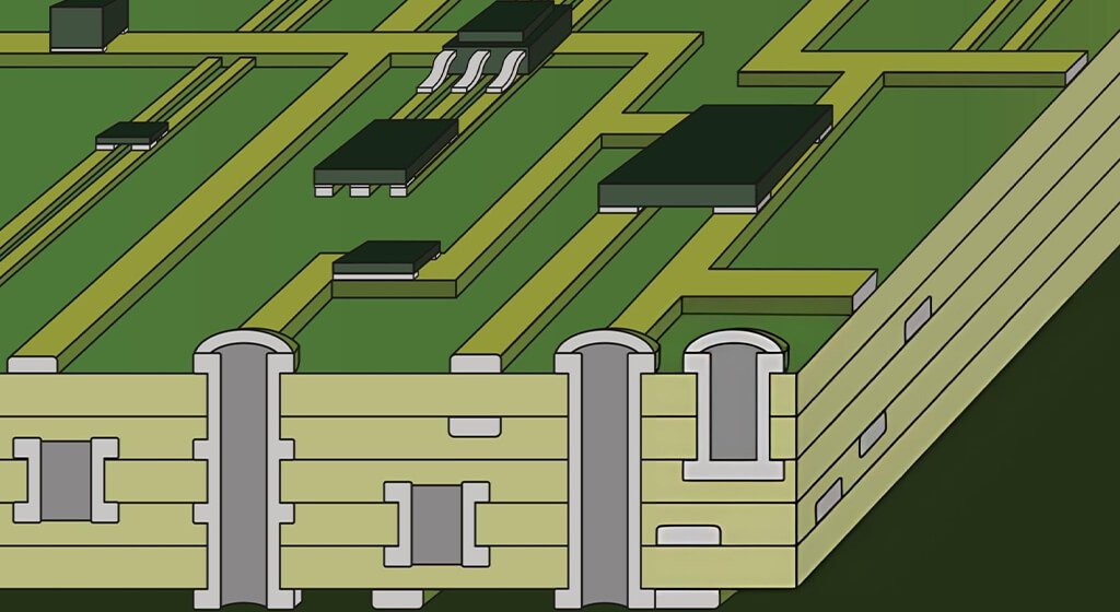
For a multilayer PCB, place important signal layers next to solid reference planes. This creates a controlled electromagnetic field between the trace and plane. It also provides a low-inductance return path.
A common high-speed stackup approach places a signal layer directly adjacent to a ground plane. The exact layer count and arrangement will depend on impedance targets, component density, voltage domains, mechanical thickness, and cost. However, the principle remains the same: every fast signal should have a continuous, nearby reference.
Use solid ground planes whenever possible. A fragmented ground plane may look organized on a CAD screen, but it can make high-frequency behavior worse. If multiple voltage domains are needed, keep the ground reference continuous and manage power domains through planes, pours, filters, and placement.
Controlled impedance also depends on stackup. Trace width alone does not define impedance. Copper thickness, dielectric thickness, dielectric constant, solder mask, trace geometry, and nearby conductors all matter.
For high-speed designs, confirm the intended stackup with your PCB manufacturer before finalizing critical trace widths. PCBSAIL’s high-speed PCB service supports stackup engineering and controlled-impedance fabrication, which helps align design intent with production capability.
6. Route High-Speed and Differential Signals for Lower EMI
Fast edge rate is often more important than clock frequency. A digital signal can create high-frequency energy far above its nominal repetition rate if its rise and fall times are short.
Route fast signals over an uninterrupted reference plane. Keep traces short where practical, but do not sacrifice return-path continuity merely to reduce a few millimeters of length.
For differential pairs, route both conductors as a pair. Maintain consistent spacing, consistent reference conditions, and reasonable length matching. Avoid sudden changes in geometry. Use symmetrical via structures when a differential pair changes layers.
Differential routing can reduce common-mode noise, but it is not a guarantee of low EMI. Any imbalance in trace length, via structure, connector pin assignment, or reference-plane transition can convert differential energy into common-mode energy. Common-mode current is particularly likely to radiate through external cables.
Avoid routing high-speed traces near board edges or connector shells without considering the return path. Also, do not assume a guard trace solves every coupling problem. A guard trace only helps when it is properly referenced and stitched to ground. Otherwise, it can become another resonant conductor.
For very fast links, reduce via stubs through back-drilling, blind vias, buried vias, or carefully planned layer transitions. These techniques can improve both signal integrity and EMI performance.
7. Design the Power Distribution Network to Reduce Noise
The power distribution network, or PDN, is a major source of EMI when it is not designed carefully.
Fast digital devices draw current in short bursts. If decoupling is poor, those bursts create voltage ripple, ground bounce, and noise that can spread through the board. The goal is to supply transient current locally and keep the current loop between the IC power pin, decoupling capacitor, and ground plane as small as possible.
Place small-value decoupling capacitors close to the power pins they support. Use short, wide connections. Connect the capacitor ground side to a solid reference plane with low-inductance vias. Do not place a capacitor close to the IC but connect it through a long, narrow route; physical proximity alone is not enough.
Use bulk capacitance to support lower-frequency load changes, but do not expect one large capacitor to solve high-frequency noise. Capacitor value, package size, mounting inductance, DC bias behavior, and placement all matter.
Switching regulators deserve extra attention. Keep the hot loop small, limit copper area on high-dV/dt switch nodes, and prevent noisy traces from coupling into feedback networks. If a converter includes an exposed pad or thermal ground, follow the recommended via and copper layout. Thermal and EMI performance are often linked.
8. Control Vias, Connectors, Cables, and Board Edges
A well-routed internal PCB can still fail an EMI test because of its interfaces.
Vias create impedance discontinuities. A single via may be harmless at low frequency, but multiple poorly planned transitions can degrade fast signals. Provide ground stitching vias around high-speed layer transitions and near connector launches. This helps maintain a continuous return-current path.
Connectors and cables deserve early attention. An external cable can become an excellent antenna, especially when common-mode current reaches it. Keep noisy circuits away from cable connectors. Place filtering, common-mode chokes, ESD protection, and shielding connections close to the entry or exit point where appropriate.
Do not route a noisy digital clock or switching node near a cable connector. Even if the product works on a bench, the cable can radiate strongly in a test chamber.
Board edges also matter. Keep high-speed or high-current routes away from edges when practical. If a ground boundary is needed near an RF or high-speed region, use via stitching to reduce edge radiation and improve shielding continuity.
9. When EMI Shielding, Filtering, and Ferrites Help
Shielding, filters, and ferrites are useful tools. They work best when they solve a known problem.
Use a metal shield can when a sensitive RF or analog circuit needs isolation from a nearby noisy circuit, or when a localized source cannot be controlled adequately by layout alone. The shield must have a good ground connection.
A floating shield or poorly stitched shield can deliver disappointing results.
Use filtering at power and cable interfaces when unwanted energy needs to be prevented from entering or leaving a section of the product. Filter placement is critical. A filter should sit at the boundary it is protecting. If noisy and clean traces run together on the same side of the filter, the noise can bypass it.
Ferrite beads can attenuate noise over specific frequency ranges. They are not universal resistors, and their behavior depends on current, DC bias, impedance-versus-frequency characteristics, and circuit conditions. Select them from measured or simulated needs, not only from a familiar part number.
A late-stage fix can be necessary, but it should not replace sound layout. The most reliable EMI strategy remains reducing the source strength and interrupting the coupling path.
10. Plan for EMC Standards and Pre-Compliance Testing
Choose the likely EMC requirements before the layout is complete. The right standard depends on product type, intended market, operating environment, ports, voltage, and radio functionality.
For multimedia equipment, IEC CISPR 32 covers Class A and Class B equipment and aims to protect radio services across 9 kHz to 400 GHz. IEC’s CISPR 32 summary also emphasizes reproducible measurement procedures.
In the United States, FCC Part 15 includes radiated-emission limits for unintentional radiators. For equipment other than Class A digital devices, the 3 m limits in 47 CFR §15.109 are 100 μV/m from 30–88 MHz, 150 μV/m from 88–216 MHz, 200 μV/m from 216–960 MHz, and 500 μV/m above 960 MHz. See the current FCC limit table.
These figures are not PCB design targets by themselves. Final compliance applies to the complete product, including its enclosure, cables, power supply, operating modes, and accessories.
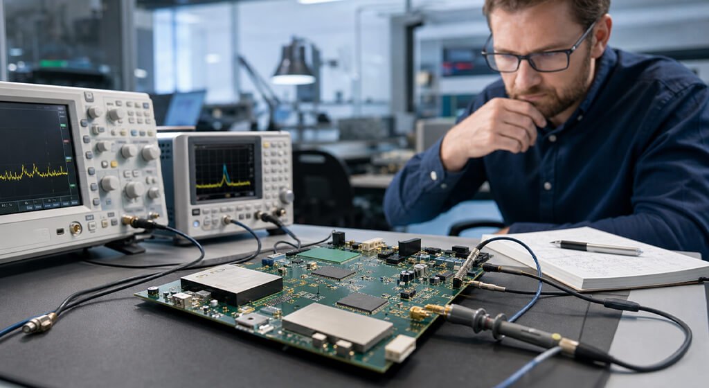
Pre-compliance testing is valuable because it finds risk before formal certification. Test the product in realistic modes. Exercise all clocks, radios, displays, motors, and interfaces. Compare operating modes, cable configurations, and power conditions. A product that is quiet while idle may become noisy during maximum data traffic or high load.
Remember that immunity matters too. IEC 61000-4-6:2023 addresses conducted immunity to RF-induced disturbances from 150 kHz to 80 MHz. IEC 61000-4-6 is a useful reminder that cables can carry interference into a product as well as out of it.
Frequency Range | FCC Radiated-Emission Limit At 3 M* | What The Design Review Should Check |
30–88 MHz | 100 μV/m | Cable routing, low-frequency switching harmonics, and large current loops. |
88–216 MHz | 150 μV/m | Clock harmonics, connector launches, and enclosure or cable resonance. |
216–960 MHz | 200 μV/m | Fast digital edges, common-mode conversion, and discontinuous return paths. |
Above 960 MHz | 500 μV/m | High-speed interfaces, via stubs, apertures, and cable radiation |
11. A Practical PCB EMI Checklist Before Fabrication
Before releasing Gerber files, review the following points:
- Are switching-regulator input loops compact?
- Are high-speed traces routed over continuous reference planes?
- Do fast signals cross plane splits, slots, or voids?
- Are return-path stitching vias present near layer transitions?
- Are decoupling capacitors connected with short, low-inductance paths?
- Are sensitive analog circuits separated from switch nodes and high-current paths?
- Are differential pairs symmetrical through vias, connectors, and reference changes?
- Are cable interfaces treated as potential antennas?
- Are filters and protection parts placed at the correct boundary?
- Has the stackup been confirmed for controlled-impedance nets?
- Are noisy traces kept away from board edges and connector launches?
- Has the complete product’s target standard and test plan been identified?
A short review at this stage can prevent repeated prototype spins later.
12. How PCBSAIL Supports EMI-Conscious PCB Builds
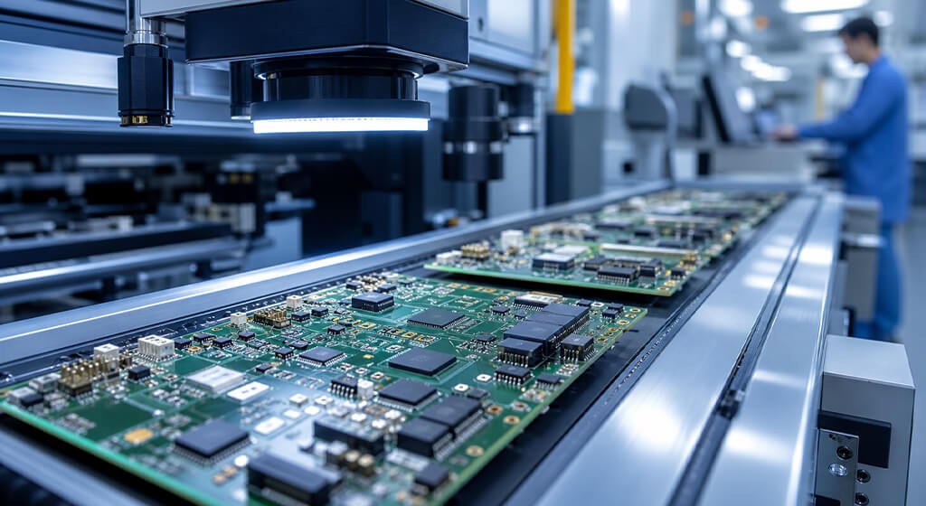
An EMI-conscious design needs manufacturing data that matches the electrical intent. Stackup construction, dielectric thickness, copper weight, impedance tolerance, via structure, and fabrication consistency all influence final board behavior.
We provides PCB fabrication and assembly services for standard FR-4, high-frequency, HDI, flexible, rigid-flex, and multilayer PCB projects. For high-speed applications, we supports controlled stackups, impedance-focused routing requirements, low-loss materials, microvias, and back-drilling options where applicable.
Learn more about high-speed PCB manufacturing and PCB fabrication and PCBA capabilities.
Before production, provide clear fabrication notes, stackup requirements, impedance targets, controlled nets, material preferences, and test expectations. A design review should confirm manufacturability without changing the electrical behavior that the EMI strategy depends on.
EMI compliance cannot be guaranteed by a bare PCB alone. It depends on the complete system. However, selecting the right stackup and manufacturing process early gives the final product a much stronger starting point.
13. FAQ About EMI in PCB Design
Can A Ground Plane Eliminate EMI?
No. A solid ground plane is one of the most effective tools for controlling return currents and reducing loop area, but it cannot eliminate every EMI source. Component placement, switching-node layout, cable interfaces, enclosure design, and filtering still matter.
What Matters More For EMI: Clock Frequency Or Rise Time?
Rise time is often more important. Fast edges contain high-frequency energy even when the nominal clock frequency is moderate. Treat signals with fast transitions as controlled transmission lines.
Should Every PCB Use Ferrite Beads For EMI Reduction?
No. Ferrite beads should be chosen for a specific noise path and frequency range. An unsuitable bead can have little effect or introduce voltage drop, resonance, or unwanted behavior in the power network.
Can A PCB Manufacturer Guarantee Final EMC Compliance?
No. Final EMC compliance is evaluated on the complete product, not only the bare board. Enclosure materials, cable length, connected accessories, power supplies, software operating modes, and system assembly all affect the result.
When Should EMI Testing Begin?
Start thinking about EMI during schematic capture and placement. Run pre-compliance testing on an early functional prototype, before production tooling and final enclosure decisions make changes expensive.
14. Conclusion
Effective PCB EMI control begins with layout discipline. Keep current loops small, preserve return paths, use a stackup with nearby reference planes, manage PDN noise, and treat cables as potential antennas. Then validate the complete product through pre-compliance and formal testing.
A design that addresses EMI from the first PCB revision is usually more reliable, easier to debug, and less costly to bring to market.