HDI PCB design becomes necessary when conventional routing can no longer meet density, size, or signal-integrity requirements. HDI PCB is common in compact medical devices, industrial controllers, network hardware, automotive electronics, and advanced consumer products.
The difficult part is rarely drawing smaller features in a layout tool. The real challenge is aligning the stackup, via structure, material system, assembly profile, and fabrication process before release.
A board can look clean in CAD and still create yield problems later. That usually happens when the design team treats HDI as a routing exercise rather than a manufacturing system.
This guide explains how to make practical HDI design decisions before sending files to fabrication.
Table of Contents
1. What Changes in an HDI PCB Design?
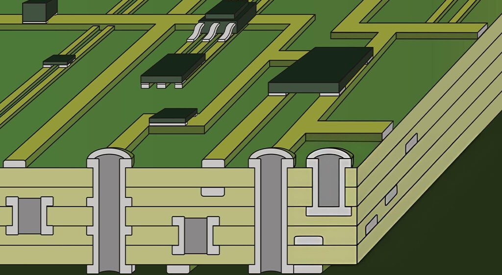
HDI stands for high-density interconnect. These boards use finer lines, smaller pads, laser-drilled microvias, blind vias, buried vias, and sequential lamination to create more routing capacity in less area.
IPC reference material defines a microvia as a blind structure with an aspect ratio of 1:1 or less. It also identifies microvias as structures with a typical diameter of 150 μm or less. IPC’s HDI reference material remains a useful starting point, although each fabricator must confirm its own qualified limits.
HDI design is often associated with smaller electronics, but size is only one reason to use it. The technology can also reduce layer transitions, shorten signal paths, improve BGA escape routing, and create more room for power distribution.
The main HDI building blocks include:
- Laser-drilled microvias between adjacent layers.
- Blind vias connecting an outer layer to an internal layer.
- Buried vias contained within the inner layers.
- Via-in-pad structures for fine-pitch BGA packages.
- Sequential build-up layers, often called SBU layers.
- Resin-filled and capped vias where the component pad requires a flat surface.
These features work together. A microvia strategy without a defined stackup usually creates confusion during DFM review.
2. When Should You Choose HDI Instead of a Standard PCB?
HDI is valuable when it solves a specific layout constraint. It should not be selected simply because a product uses a modern processor or BGA package.
A standard multilayer PCB may be the better choice when the board has sufficient area, moderate pin density, and comfortable routing channels. Conventional through-hole vias remain more economical and simpler to manufacture.
Design Condition | HDI May Be Justified | A Conventional PCB May Be Sufficient |
Fine-Pitch BGA | Escape channels are blocked by pad density | Fanout fits with standard vias |
Board Size | The enclosure cannot grow | More board area is available |
Layer Count | Routing requires excessive layers | Routing completes with practical layers |
High-Speed Signals | Via stubs and long paths become problematic | Signal paths remain controlled |
Product Volume | Performance and space support added cost | Cost pressure outweighs density benefits |
Rework Strategy | Assembly process supports HDI structures | Rework requirements favor simpler structures |
The right question is not, “Can we build this as HDI?” The better question is, “What problem does HDI solve that a standard stackup cannot?”
For example, a fine-pitch processor may need HDI only around the BGA. The rest of the board may still follow conventional routing rules. That hybrid approach often controls cost without sacrificing routing flexibility.
If the design also needs additional routing layers, review the basics of multilayer PCB construction before committing to a build-up structure.
3. HDI PCB vs. Standard Multilayer PCB
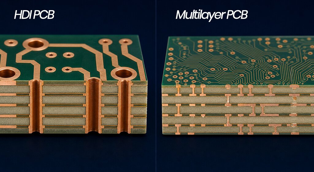
HDI and standard multilayer boards can look similar from outside. Their internal routing strategy and manufacturing process are very different.
A standard multilayer board typically relies on mechanically drilled through-holes and conventional lamination. HDI boards often add laser-drilled microvias, thin buildup dielectrics, and sequential lamination cycles.
Feature | Standard Multilayer PCB | HDI PCB Design |
Main Interconnect | Through-hole vias | Microvias, blind vias, buried vias, or via-in-pad |
Routing Density | Moderate | Higher, especially near dense packages |
Stackup Process | Conventional lamination | Often sequential buildup |
BGA Breakout | Limited by through-hole geometry | More routing options through microvias |
Manufacturing Complexity | Lower | Higher due to extra process control |
Inspection Focus | Standard structural and electrical checks | Additional attention to via interfaces and registration |
Cost Drivers | Layer count, material, copper weight | Plus buildup cycles, laser drilling, filling, plating, and testing |
The right comparison is not “cheap versus expensive.” The better question is whether HDI reduces a larger system-level problem.
For example, HDI may prevent a larger enclosure, eliminate unnecessary routing layers, or create feasible breakout paths for a dense processor. In another project, it may simply add cost without creating a real technical advantage.
If your design remains feasible using conventional construction, review multilayer PCB manufacturing options before committing to sequential buildup technology.
4. Choose the Stackup Before Starting Dense Routing
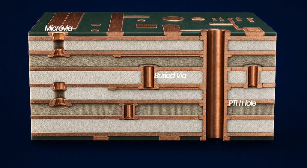
The stackup is the foundation of HDI PCB design. It determines the available via transitions, impedance geometry, copper distribution, drilling sequence, and lamination cycles.
A common mistake is routing first and asking for a stackup later. That approach often leads to unroutable BGA fanouts, unrealistic microvia targets, or impedance changes that force a redesign.
Most HDI boards use one of these build-up concepts:
Stackup Concept | Typical Use | Main Consideration |
1+N+1 | One build-up layer on each side | Suitable for moderate BGA escape needs |
2+N+2 | Two build-up layers on each side | Adds routing flexibility and cost |
Asymmetric HDI | Density is concentrated on one side | Requires careful warpage control |
Any-Layer HDI | Dense interconnection across many layers | Requires advanced fabrication capability |
In a 1+N+1 structure, the outer layers are added after the core is built. Laser microvias can connect L1 to L2 and the opposite outer layer to its adjacent internal layer.
A 2+N+2 structure adds another sequential lamination cycle. It creates more routing channels, but it also increases fabrication complexity, material movement, and process risk.
Before approving a stackup, give the fabricator the following information:
- Maximum BGA pitch and package type.
- Expected layer count and board thickness.
- Controlled-impedance requirements.
- Highest operating frequency or edge rate.
- Copper weight by layer.
- Thermal and mechanical constraints.
- Via-in-pad requirements.
- Assembly temperature profile, if known.
The stackup should also support the return path of every critical signal. A fast trace routed over a split reference plane can create more problems than a longer, properly referenced route.
5. Plan BGA Escape Routing and Via Architecture Together
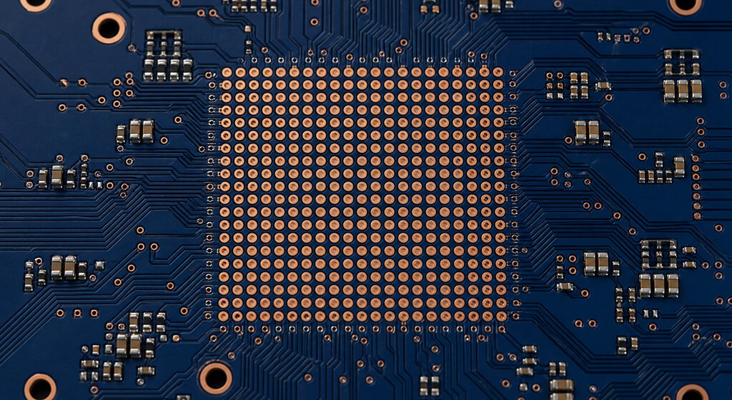
BGA escape routing is often the first reason engineers consider HDI. Fine-pitch packages leave limited space between pads, especially when the design requires power, ground, high-speed interfaces, and multiple memory channels.
The via structure must be selected with the BGA geometry in mind. A conventional through-hole via may consume too much routing space and introduce an unnecessary stub.
Microvias can create a direct path from an outer BGA pad to the first internal routing layer. This arrangement may free inner routing channels and allow shorter connections to nearby reference planes.
Via-in-pad plated over, or VIPPO, is frequently used for dense BGA layouts. The process fills the via, caps it, and creates a flat pad surface for assembly. It can improve routing access, but it must be planned as a fabrication feature from the beginning.
Do not place ordinary open vias in BGA pads and assume solder paste will behave normally. Unfilled vias can pull solder away from the joint during reflow, creating insufficient solder volume or hidden assembly defects.
A useful BGA planning sequence looks like this:
- Confirm the package pitch, ball map, and recommended land pattern.
- Identify high-speed, power, ground, and low-speed escape zones.
- Select microvia, stacked-via, or staggered-via structures with the fabricator.
- Reserve nearby reference planes for critical signal layers.
- Check assembly clearances before finalizing the pad field.
- Run a DFM review before expanding the routing pattern across the board.
Stacked microvias can reduce horizontal routing distance, but they require tighter process control. Staggered microvias may offer a more forgiving structure where density permits.
The choice should reflect available space, reliability requirements, and the selected fabricator’s qualified process window.
6. Set HDI Design Rules From Fabricator Data

Generic internet rules are helpful for early estimates, but they are not manufacturing specifications. Every HDI supplier has different capability limits, qualified materials, laser drilling processes, and plating controls.
Ask for a current capability table before locking any of these values:
- Minimum laser-drilled microvia diameter.
- Minimum capture-pad diameter.
- Allowed microvia depth and aspect ratio.
- Minimum trace width and spacing.
- Copper thickness on build-up layers.
- Via fill requirements.
- Registration tolerances.
- Maximum sequential lamination cycles.
- Approved material systems.
IPC-6012F covers qualification and performance requirements for rigid printed boards, including boards using blind vias, buried vias, and microvias. The revision also expanded attention to reliability and verification issues. IPC’s IPC-6012F release is useful context when defining supplier requirements.
Microvias deserve special attention because their quality depends on several connected processes. Laser drilling, desmear, metallization, copper plating, resin behavior, and thermal exposure all influence long-term performance.
IPC issued an industry warning after reports of latent microvia failures in certain high-performance applications. Those failures could emerge during reflow exposure and may not be visible through room-temperature inspection alone. IPC’s microvia reliability warning is a reminder to discuss reliability expectations early.
This does not mean microvias are inherently unreliable. It means the design, material, fabrication process, and test method must be treated as one qualified system.
7. Control Signal Integrity, Power Delivery, and Heat
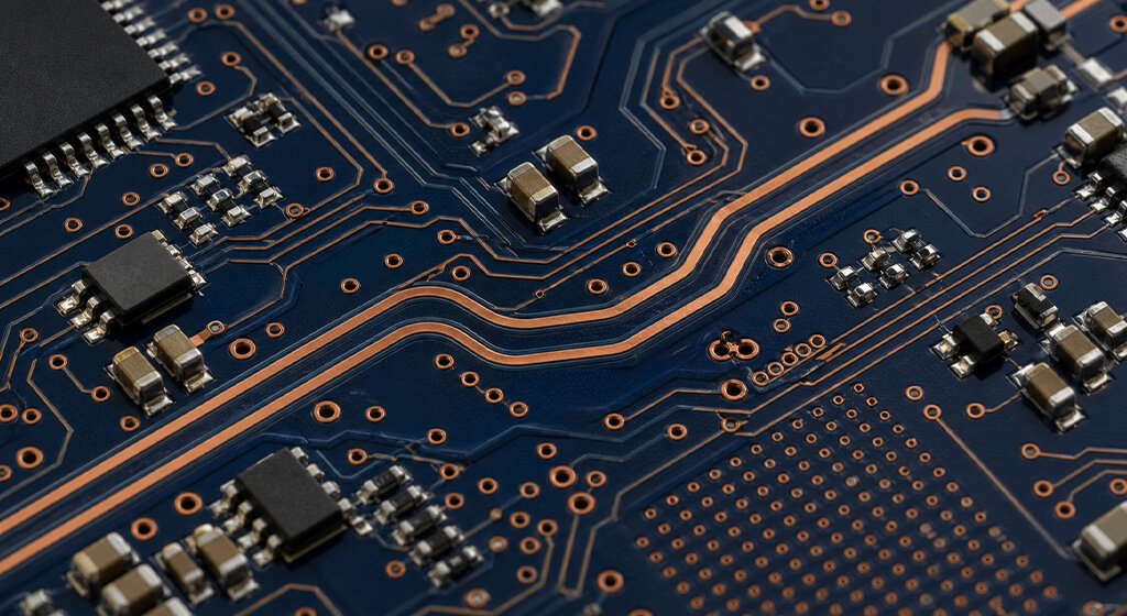
HDI creates routing freedom, but it does not remove electrical constraints. Smaller geometries often make stackup choices more important because trace widths, dielectric thicknesses, and reference planes become tightly connected.
For high-speed nets, focus on three areas:
- Continuous return paths.
- Stable impedance geometry.
- Controlled transitions between layers.
A signal does not travel alone. Its return current follows the nearest suitable reference plane. When a trace crosses a plane split, changes layers without a nearby return path, or encounters a poor via transition, the signal path becomes less predictable.
High-speed designs often need back-drilling, via optimization, impedance modeling, or carefully selected layer transitions. The requirements depend on the protocol, channel length, connector design, and component edge rate.
If your board includes high-speed interfaces, coordinate the HDI structure with high-speed PCB design requirements before routing differential pairs.
Power-delivery design also changes in compact HDI boards. Dense processors and memory devices may demand low-impedance power paths, local decoupling, and closely coupled power-ground planes.
Do not assume that adding more copper automatically solves thermal problems. Thick copper can affect etching, lamination, drilling, and warpage. The right thermal strategy often combines copper balance, thermal vias, component placement, plane design, and enclosure-level heat removal.
8. Build DFM and Reliability Into the Release Package
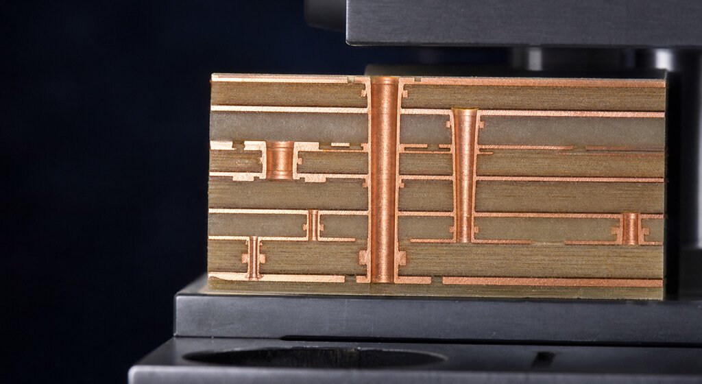
A complete release package helps the fabricator identify risks before production starts. Gerber files alone are rarely enough for a complex HDI design.
Your release package should include:
- Fabrication drawings with controlled dimensions.
- Layer stackup and material callouts.
- Drill files and drill map.
- Blind, buried, and microvia requirements.
- Impedance table and coupon requirements.
- Netlist, where available.
- Via fill, cap, and surface-finish requirements.
- IPC acceptance class, if applicable.
- Assembly drawing and pick-and-place data.
- Known critical nets, packages, and design constraints.
A fabricator should review the design for annular ring, registration, drill depth, copper balance, impedance geometry, soldermask clearance, and assembly compatibility.
Thermal stress should also be part of the conversation. IPC-TM-650 Method 2.6.27 provides a framework for assessing a board’s ability to withstand assembly and rework thermal excursions. IPC’s thermal-stress test guide explains the method’s purpose and approach.
NASA and JPL also studied microvia behavior under thermal and reflow cycling. Their work examined filled and unfilled microvias, daisy-chain structures, and cross-sections under defined test conditions. The NASA/JPL study should not be treated as a universal pass-fail rule, but it illustrates why test conditions matter.
For assembled boards, fabrication and assembly teams should work from the same assumptions. PCBSAIL’s SMT assembly service can be considered alongside fabrication requirements when the design includes fine-pitch BGAs, bottom-terminated components, or via-in-pad structures.
9. Understand the Cost and Lead-Time Drivers
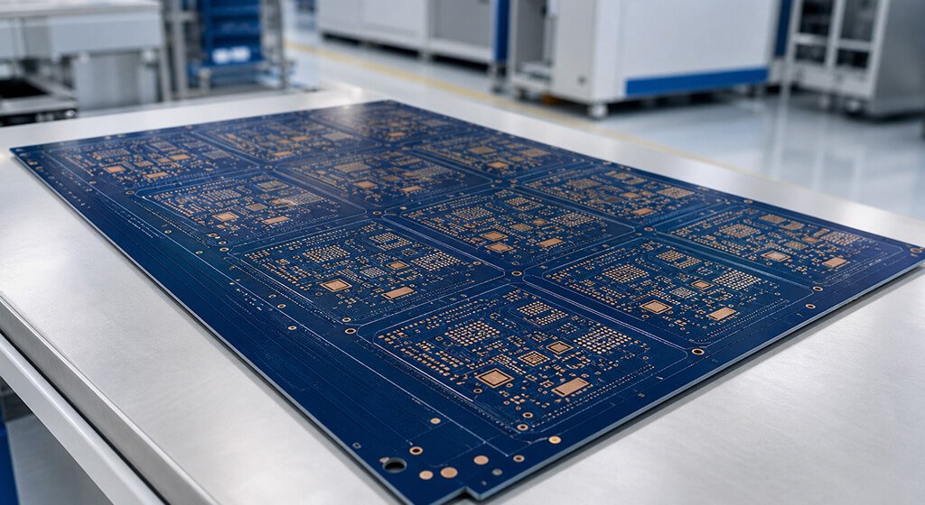
HDI cost is shaped by process complexity, not only board area or layer count. A small board can still cost more than a larger conventional board if it requires multiple lamination cycles and filled microvias.
The main cost drivers include:
- Number of sequential laminations.
- Quantity and depth of microvias.
- Stacked versus staggered microvias.
- Via filling and capping requirements.
- Fine-line imaging requirements.
- Controlled-impedance complexity.
- Material selection.
- Yield sensitivity from tight registration targets.
- Inspection and reliability requirements.
The most expensive HDI feature is often the one that was added late. A routing change near the end of a project can force another build-up layer, a more complex via structure, or a revised assembly approach.
Early stackup review is therefore a cost-control measure, not just an engineering checkpoint.
Try to avoid specifying advanced structures where a simpler alternative works. For example, a staggered microvia may meet the routing need without the added complexity of a stacked arrangement.
10. Prepare an Effective HDI Design Review
A useful HDI design review is specific. Instead of asking whether a board is “manufacturable,” ask questions that expose actual process limits.
Examples include:
- Is the selected microvia diameter qualified for this material and build-up layer?
- Can the proposed BGA escape pattern meet registration tolerances?
- Does the stackup support the required impedance without impractical trace widths?
- Are stacked microvias necessary, or can staggered structures work?
- Does via-in-pad require resin filling and copper capping?
- Is copper distribution balanced enough to manage warpage?
- Can the assembly process support the selected pad and via structures?
- What coupon, cross-section, or thermal-stress verification is appropriate?
The best time for this review is before component placement and routing become difficult to change.
PCBSAIL’s HDI PCB manufacturing provides a starting point for discussing stackup optimization, material selection, microvias, and via-in-pad requirements. Bring the BGA data, preliminary layer count, critical nets, and electrical targets to that discussion.
For projects requiring both board fabrication and assembly coordination, a turnkey PCBA workflow can reduce handoffs between separate suppliers.
11. FAQ About HDI PCB Design
When Does A 1+N+1 HDI Stackup Make Sense?
A 1+N+1 stackup is often suitable when the design needs one additional routing layer near each outer surface. It can support moderate BGA escape routing without the complexity of multiple build-up cycles.
It is usually a sensible starting point when one microvia layer solves the density problem.
Does Via-In-Pad Always Solve BGA Routing Problems?
Via-in-pad can provide valuable routing access under dense BGA packages. However, it adds fabrication and assembly requirements, especially when vias must be filled, capped, and planarized.
It should be used where the routing benefit justifies the additional process complexity.
Does HDI Always Reduce The Total Layer Count?
No. HDI can reduce layer count in some designs, but that is not guaranteed. A compact board may still need many layers for power distribution, impedance control, shielding, or thermal performance.
HDI often improves routing access more than it reduces total layers.
What Should Be Included In An HDI DFM Package?
It included the complete stackup, material requirements, via structures, impedance table, drill data, fabrication drawing, assembly information, and acceptance criteria.
Also identify critical BGA packages, high-speed nets, and any area where a process change could affect function or reliability.
12. Final Takeaway
HDI PCB design works best when it begins with manufacturing reality. Select the stackup early, define via structures with the fabricator, and connect routing decisions to assembly and reliability requirements.
The smallest feature on the board often has the largest effect on yield. Treat microvias, BGA escape routing, materials, and thermal exposure as connected decisions from the first layout review.
Get a PCB Quote