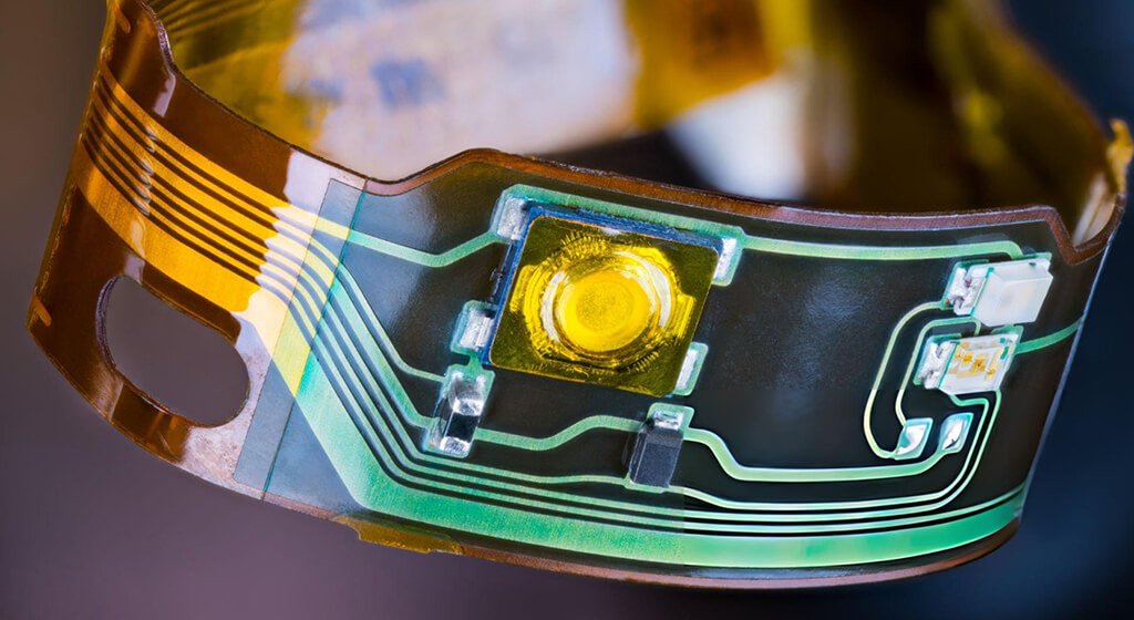

SMT defects in PCB assembly can short a circuit, interrupt a signal path, or weaken a joint that later fails in service. A board may also pass a quick visual check while hiding a poor connection beneath a package.
Surface-mount technology places components directly on printed pads before reflow forms the solder joints. It enables dense, automated builds, but it leaves little tolerance for poor paste control, placement error, or uneven heating.
This article will help you learn 15 common SMT defects and match the inspection images supplied with this article.
Table of Contents
1. What Counts as an SMT Defect?

SMT defects is any departure from the intended paste deposit, component position, solder joint, or component condition. Some are visible at the line; others appear only in X-ray images or electrical test results.
Acceptance depends on the product, package, circuit function, and documented class requirements. A minor visual irregularity on one consumer board may be unacceptable in a medical, industrial, or automotive application.
Set the acceptance basis before production starts, so disposition decisions remain consistent throughout the build. IPC-A-610 covers electronic-assembly acceptability, while IPC J-STD-001 covers soldering processes and materials.
SMT Defect | Typical Risk | First Control Point |
Solder Bridging | Short circuit | Paste volume, stencil, placement |
Tombstoning | Open circuit | Pad symmetry, thermal balance, reflow |
Missing Component | Functional failure | Feeder control, first article, AOI |
Misaligned Component | Open, short, or weak joint | Placement accuracy, fiducials |
Insufficient Solder | Weak or open connection | Paste deposit, wetting, stencil |
Excess Solder | Bridging or solder balls | Aperture design, paste control |
Cold Solder Joint | Intermittent or weak connection | Reflow profile, cleanliness |
Open Solder Joint | Open circuit | Placement, coplanarity, wetting |
Solder Splash | Short or contamination risk | Paste handling, reflow, cleanliness |
Polarity Reversal | Functional failure or damage | BOM, centroid, first article |
Lifted Component | Open or weak joint | Coplanarity, placement, reflow |
Damaged Component | Latent or immediate failure | Handling, feeder setup, rework |
Voiding | Reduced thermal or mechanical reliability | Reflow, moisture, pad design |
Non-Wetting | Unreliable electrical connection | Surface condition, paste, profile |
Wrong Component | Incorrect circuit behavior | BOM control, traceability, inspection |
2. Why SMT Defects Happen?
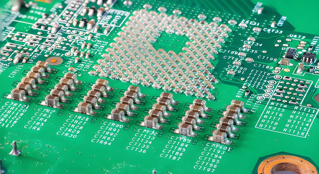
Defects rarely have one cause. A bridge found after reflow may begin with a stencil aperture, a placement offset, or an unsuitable pad layout. Starting at the oven can therefore send the investigation in the wrong direction.
Begin with the release package and materials, because those inputs set the limits for every downstream process. Incorrect footprints, vague polarity markings, conflicting BOM data, oxidized pads, and unsuitable packaging can create failures before the board reaches the line.
Paste printing is the first major process gate, because every solder joint begins with its deposit. Stencil thickness, aperture geometry, board support, printer registration, paste condition, and cleaning frequency determine the volume that reaches every pad.
Placement adds another layer of risk, particularly on fine-pitch and very small packages. Feeder faults, poor fiducial recognition, the wrong nozzle, excessive placement force, or outdated centroid data can shift, damage, or omit components.
Reflow determines how those deposits become joints, and small thermal differences can alter the result. Ramp rate, soak, peak temperature, time above liquidus, component mass, and local copper all influence wetting and joint formation.
Handling and inspection complete the picture and can undo earlier process control. Board flex, careless depaneling, poorly controlled rework, and inadequate test coverage can either create a defect or let one escape.
The SMT assembly workflow shows where those controls sit in a production line. Root-cause work should always trace the defect back to the earliest stage that can prevent it.
3. The 15 Common SMT Defects
3.1. Solder Bridging
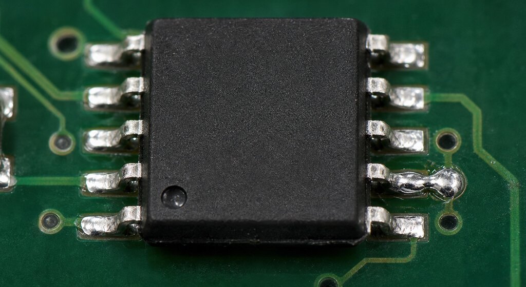
Solder bridging is unintended solder between adjacent pads, leads, or conductors. On fine-pitch devices, even a small bridge can short a supply rail or signal line.
Look first at paste volume, stencil apertures, paste slump, placement offset, and solder-mask clearance. Confirm those inputs with SPI before changing the reflow profile, which isolates printing problems from oven behavior.
3.2. Tombstoning
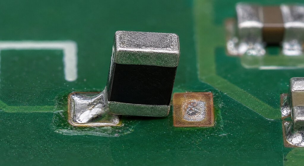
Tombstoning occurs when one end of a small chip component lifts during reflow. The part stands upright or tilts sharply, leaving one termination disconnected.
Uneven wetting forces are usually responsible, especially on small passive parts. One end may reach wetting temperature first because of asymmetric pads, unequal copper, inconsistent paste deposits, or placement offset.
Small 0402, 0201, and 01005 passives are particularly sensitive. Review pad symmetry and thermal balance during DFM, before the design reaches production.
3.3. Missing Component
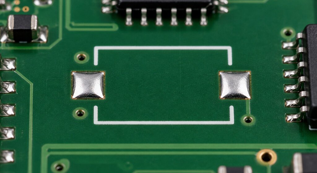
A missing component leaves an intended location vacant after assembly. Typical causes include an empty feeder, pickup failure, vision rejection, bad program data, or a part that detached during reflow.
The impact can be obvious or subtle, depending on the circuit. Feeder checks, first article inspection, AOI, and functional testing provide useful overlapping controls.
3.4. Misaligned Component
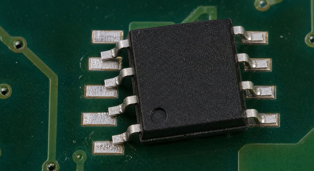
A misaligned component sits off-center, rotated, or shifted from its intended pads. Severe movement can leave leads partly unsupported or bridge fine-pitch pads.
Check fiducials, board support, placement offsets, nozzle condition, and part geometry. When one package shifts repeatedly at one location, inspect the local pad design and paste balance.
3.5. Insufficient Solder
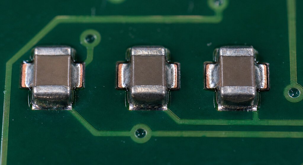
Insufficient solder leaves too little alloy to form a reliable fillet. The connection may pass a basic continuity check, then fail under vibration, thermal cycling, or mechanical stress.
Blocked apertures, poor paste release, excessive aperture reduction, weak wetting, and solder wicking are common causes. SPI should catch an under-volume deposit before reflow.
3.6. Excess Solder
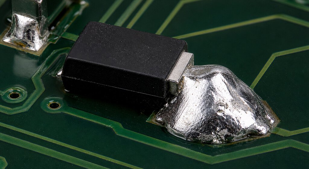
Excess solder is an oversized deposit around a lead or termination. It can conceal the joint shape, form solder balls, or flow onto neighboring pads.
Excess printed volume is the usual source, although displacement and reflow behavior can worsen it. Review aperture size and stencil thickness before blaming line operators.
3.7. Cold Solder Joint
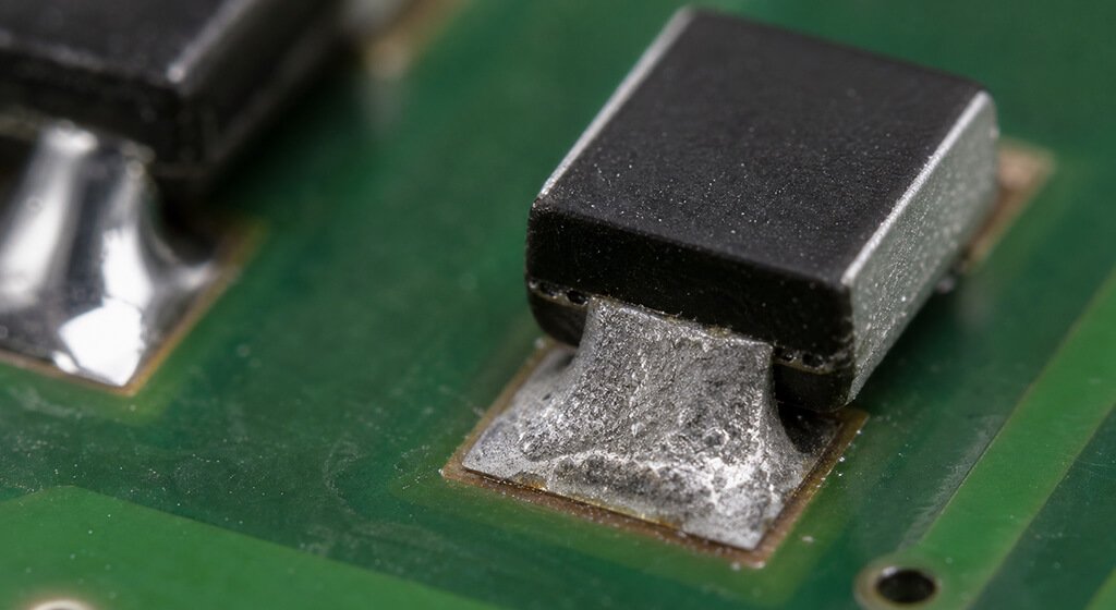
A cold solder joint often looks dull, rough, grainy, or poorly fused. It lacks the smooth, well-wetted profile expected from a sound connection.
Insufficient heat, contamination, oxidation, expired paste, weak wetting, and a poor profile can all contribute. Visual inspection flags the condition, while electrical testing shows whether it is already unstable.
3.8. Open Solder Joint
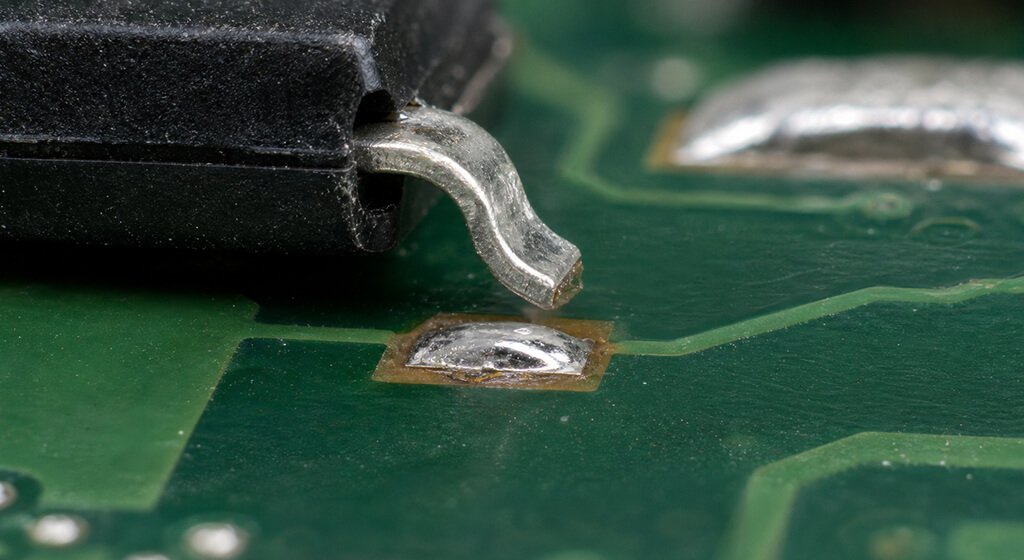
An open solder joint has no reliable electrical path between a component termination and its pad. Solder may be visible, yet a physical or hidden gap prevents continuity.
Common causes include placement height, poor coplanarity, insufficient paste, non-wetting, lead damage, and board warp. Confirm the joint condition visually, then verify the circuit impact with ICT or functional test.
3.9. Solder Splash

Solder splash is unintended solder beads or spatter on the board surface. Small balls can lodge between conductors, create intermittent shorts, or complicate coating and inspection.
Moisture, excess paste, poor stencil cleaning, inadequate board support, rapid outgassing, and aggressive reflow can contribute. Check paste handling and the ramp profile, then inspect the stencil underside.
3.10. Polarity Reversal
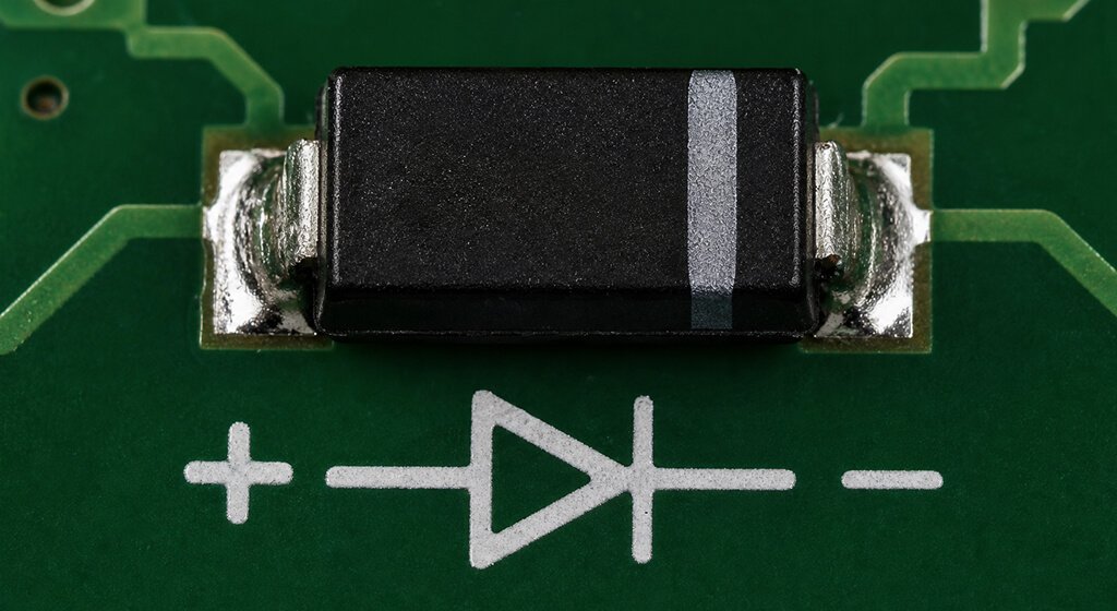
Polarity reversal occurs when an orientation-sensitive component is mounted in the wrong direction. Diodes, LEDs, electrolytic capacitors, connectors, and many ICs can fail or misbehave when reversed.
This is usually a data-control failure, not a soldering failure. The BOM, centroid file, assembly drawing, silkscreen, component marking, and first article should all match the released revision.
3.11. Lifted Component
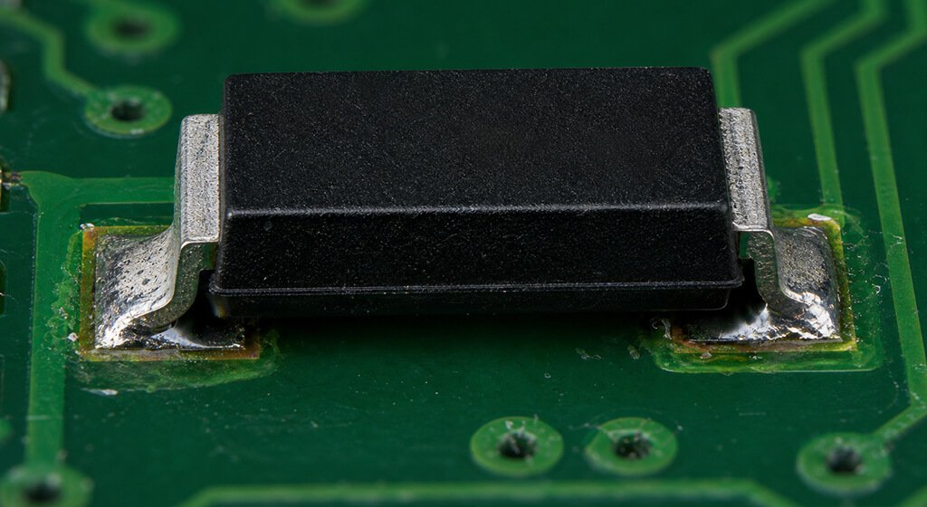
A lifted component has one or more terminations raised from the intended pad. Unlike a tombstone, the part may remain horizontal while a lead or end termination loses contact.
Poor coplanarity, low placement force, uneven wetting, board warp, or later handling can cause it. Inspect the component body and every joint, because one lifted end can produce an intermittent open.
3.12. Damaged Component
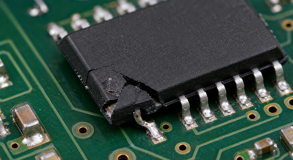
A damaged component may show cracked molding, chipped ceramic, bent leads, damaged terminations, or heat-related package degradation. Damage can occur during incoming handling, feeder setup, placement, rework, or depaneling.
A good solder joint does not prove that the component survived. Incoming inspection, correct nozzle selection, controlled rework, and post-assembly test matter most for moisture-sensitive or brittle parts.
3.13. Voiding
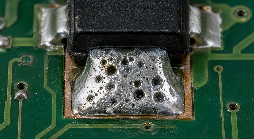
Voiding is the presence of cavities inside a solder joint. It matters beneath thermal pads, power packages, QFNs, and BGAs because voids can reduce heat transfer and mechanical support.
Moisture, flux outgassing, paste chemistry, pad design, via-in-pad treatment, and reflow conditions affect void formation. X-ray is normally required because significant cavities are hidden beneath the component.
For assemblies with bottom-terminated packages or dense ball arrays, plan inspection before release. The BGA assembly guide is a useful starting point for matching package risk with process and inspection choices.
3.14. Non-Wetting
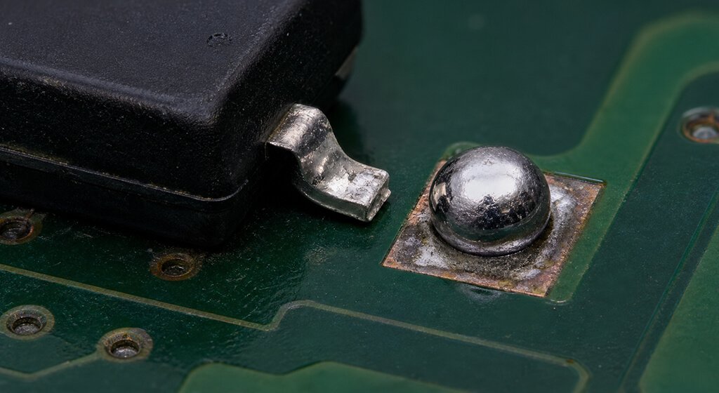
Non-wetting occurs when molten solder fails to spread and bond to the pad or component termination. The alloy may form a rounded bead instead of a continuous connection.
Oxidized surfaces, contamination, expired paste, unsuitable flux activity, incompatible finishes, and poor thermal conditions can cause it. Check solderability and cleanliness first, then review the profile against the paste and assembly stackup.
3.15. Wrong Component
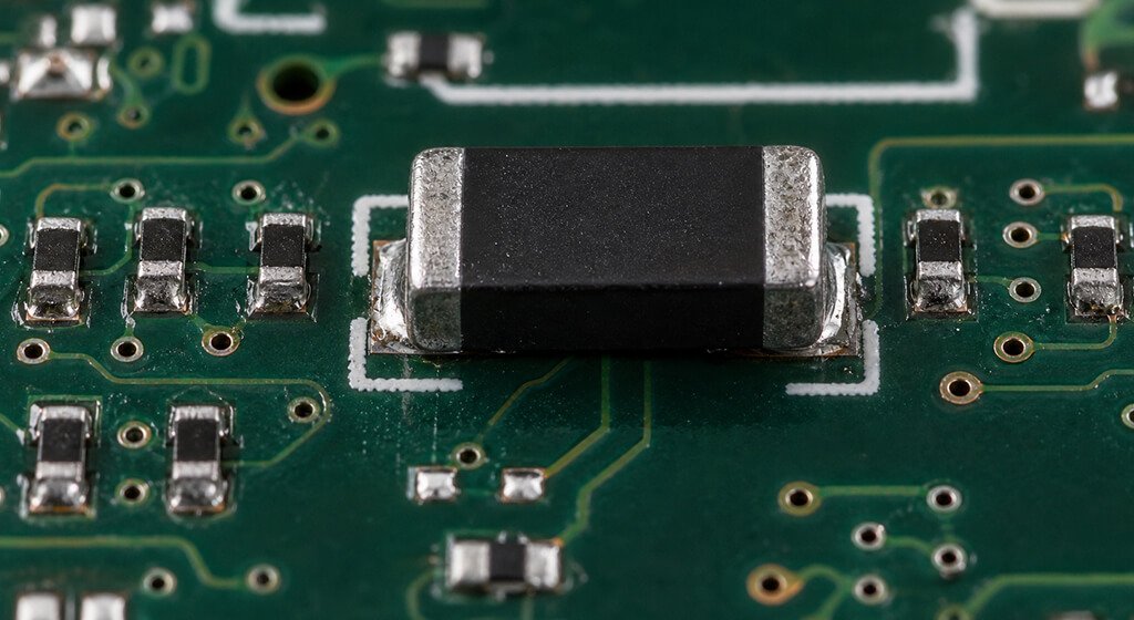
A wrong component has the incorrect value, package, manufacturer part number, or functional type for a reference designator. The board may look fine while producing the wrong voltage, timing, impedance, or firmware behavior.
Prevent it through strict BOM control. Approved alternates, manufacturer part numbers, feeder labels, barcode traceability, first article inspection, and electrical test must agree before volume production starts.
4. Preventing Defects Before Reflow
The cheapest defects never reach the printer. Prevention starts with a design and documentation review before material is bought or a stencil is ordered.
4.1. Compare Every Footprint With The Component Datasheet
Compare every footprint with the component datasheet, particularly for fine-pitch, bottom-terminated, thermal-pad, and very small passive packages.
Check pad symmetry, mask clearance, paste apertures, thermal reliefs, fiducials, and local spacing.
4.2. Reconcile The Released Design Package
Reconcile the released design package next, rather than resolving contradictions at the line. Gerbers or ODB++, the BOM, approved alternates, centroid data, assembly drawings, polarity notes, and revision history must describe the same build.
4.3. Material Manage
Material discipline is aslo important because poor inputs cannot be corrected by inspection.
Confirm the board finish, component packaging, moisture sensitivity, paste storage, paste working life, and stencil condition before the line begins.
4.4. SPI Test
During production, use SPI to find deposit-volume and registration problems before placement. First article inspection should confirm part number, value, orientation, position, and workmanship before the lot is released.
4.5.Temperature Profile est
Profile an actual representative board rather than trusting oven setpoints alone, especially after a material or layout change.
Thermal mass, copper distribution, package mix, and component height determine the temperatures the assembly actually sees.
4.6. Contingency Plan
Define the response to a repeated defect in advance, before production pressure influences the decision. The team should know when to stop the line, isolate boards, collect evidence, review process data, and approve a corrective action.
5. Match Inspection to the Failure Mode
Inspection should follow the failure mode, not a generic equipment checklist. No single method can confirm every part of a completed PCBA.
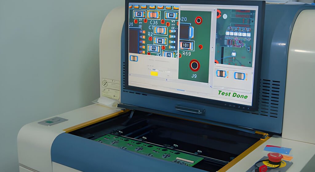
SPI measures paste deposits before components are placed and before reflow obscures the evidence. It identifies volume, height, area, and registration problems that later become bridges, insufficient solder, or placement-related failures.
AOI works well for visible conditions: missing parts, polarity errors, tombstones, shifted components, bridges, and many joint-shape abnormalities. It cannot reliably judge solder joints hidden beneath BGA or QFN bodies.
Use X-ray when hidden joints, voiding, BGA bridges, or bottom-terminated package connections carry meaningful risk. Specify it because the package and application require it, not because it sounds comprehensive.
ICT and flying-probe testing identify opens, shorts, and some component-value errors. Functional testing confirms whether the completed assembly performs its required task under defined conditions.
For complex builds, assemble the inspection plan around actual failure risks and acceptance requirements. Our turnkey PCBA can bring sourcing, assembly, inspection, and test requirements into one release discussion.
6. Questions to Ask a PCB Assembly Partner
Before placing a prototype or production order, you can ask how the supplier controls the risks in your design. Broad quality claims are not enough; the answers should describe specific controls and records.
Ask whether stencil apertures and paste deposits are reviewed at fine-pitch locations. Ask how the reflow profile is verified, how first articles are approved, and when AOI or X-ray is justified.
For BGA, QFN, and thermal-pad packages, ask how hidden joints are inspected and documented. For polarity-sensitive assemblies, ask how the BOM, centroid data, and visual orientation checks are reconciled.
Ask what happens when a defect appears. A credible answer includes traceability, containment, root-cause analysis, documented corrective action, and a check that the fix did not introduce another problem.
7. Frequently Asked Questions
What Causes Solder Bridging In SMT Assembly?
Solder bridging usually begins with excess or misplaced paste. Oversized stencil apertures, paste slump, placement offset, inadequate solder-mask clearance, and uncontrolled solder flow can combine to create a short.
Is AOI Enough For SMT Defect Inspection?
AOI is valuable for visible placement and solder defects, but it cannot prove hidden-joint quality. BGA, QFN, voiding, electrical continuity, and functional behavior may require X-ray, ICT, flying-probe, or functional testing.
Which SMT Defects Require X-Ray Inspection?
Voiding beneath thermal pads, BGA bridges, hidden BGA opens, and many QFN-joint concerns require X-ray. The inspection plan should reflect the package, reliability target, and consequences of an escaped defect.
What Information Should Be Supplied Before SMT Assembly Begins?
Provide released PCB data, a BOM with manufacturer part numbers, approved alternates, centroid data, assembly drawings, polarity notes, revision control, and defined test requirements.
Incomplete documentation is a preventable source of wrong parts and orientation errors.
8. Build Defect Prevention Into the Release Package
Reliable assemblies are built through prevention, not final visual inspection alone. Clear data, balanced pad geometry, controlled paste printing, accurate placement, measured reflow, and risk-based testing do more than late-stage rework ever can.
For a new board, prepare the Gerbers or ODB++, BOM, pick-and-place data, assembly drawings, test requirements, and critical-to-quality notes. Our SMT assembly service can help you identify manufacturing risks while design changes are still inexpensive.