
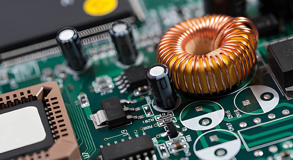
Modern electronics depend on small, repeatable connections between components and copper pads. That is why “SMT components” appears frequently in design reviews, BOM discussions, and assembly quotations.
The phrase is useful, but it can blur an important distinction. SMT means Surface Mount Technology, which is the manufacturing method. SMD means Surface Mount Device, which is the physical component mounted on the board.
In everyday engineering conversations, people often use “SMT components” to describe SMD resistors, capacitors, ICs, diodes, connectors, and other surface-mount parts. That usage is understood across the industry, provided the design files, BOM, and manufacturing notes use precise terminology.
Selecting SMT components is not only about fitting more circuitry into a smaller board. The component package affects placement accuracy, solder-joint inspection, rework options, sourcing risk, and long-term product support.
This guide explains the main categories of SMT components, the packages engineers encounter most often, and the decisions that shape a reliable assembly.
Table of Contents
1. SMT vs. SMD vs. Through-Hole: What Is the Difference?
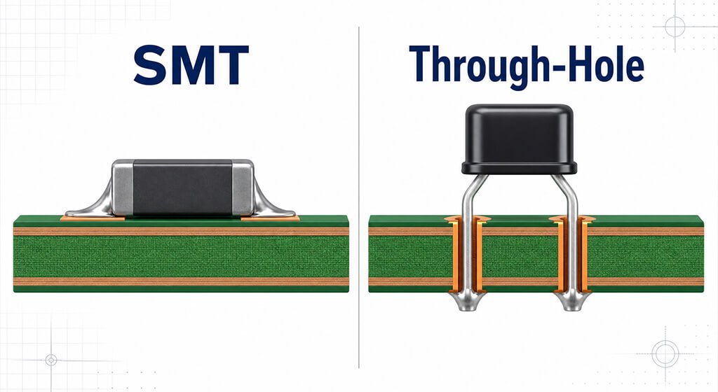
Before comparing packages, it helps to separate the process from the part.
Term | What It Describes | Example |
SMT | Which is process that the mount was put on PCB pads | Solder paste printing, pick-and-place, reflow |
SMD | A device designed for surface mounting | 0603 resistor, QFN IC, BGA processor |
THT | Through-hole technology, where leads pass through drilled holes | Pin headers, large capacitors, power connectors |
SMT places components directly on pads located on the PCB surface. The process normally uses solder paste, automated placement equipment, controlled reflow, inspection, and electrical testing.
Through-hole technology remains useful when a component needs strong mechanical retention. Connectors, transformers, switches, and heavy power devices often benefit from plated-through-hole mounting. Many practical boards therefore use mixed technology rather than choosing only SMT or only through-hole assembly.
The best approach depends on the product’s electrical demands, mechanical environment, assembly volume, service requirements, and component availability. A compact consumer device may favor dense SMT placement, while an industrial controller may combine SMT ICs with through-hole power connectors.
2. Main Types of SMT Components
SMT packages can contain almost every function found in a modern circuit. The package tells you how the device mounts, but the electrical role still determines whether it belongs in the design.
2.1. Passive Components
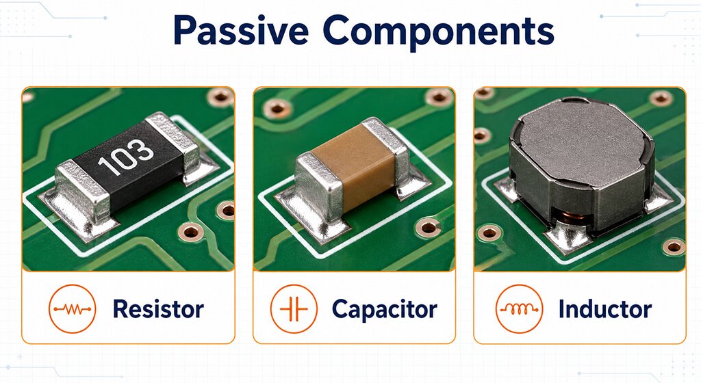
Passive components do not amplify or switch signals. They manage current, voltage, filtering, timing, impedance, and stored energy.
Common passive SMT components include:
- Resistors for current limiting, pull-up or pull-down functions, voltage division, and termination.
- Capacitors for decoupling, filtering, timing, coupling, and energy storage.
- Inductors for filtering, power conversion, and RF circuits.
- Ferrite beads for controlling unwanted high-frequency noise.
- Thermistors and fuses for sensing temperature or protecting circuits.
Chip resistors and multilayer ceramic capacitors are among the most common parts in SMT assembly. Their small size supports dense layouts, but the smallest packages need accurate pad geometry and a controlled soldering process.
2.2. Active Components
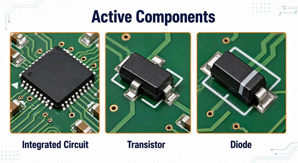
Active components control, amplify, convert, or process electrical signals. They usually require a power source and demand more attention during selection.
Typical active SMT devices include:
- Diodes for protection, rectification, and voltage regulation.
- Transistors and MOSFETs for switching or amplification.
- Voltage regulators and power-management ICs.
- Microcontrollers, processors, memory devices, and communication ICs.
- Sensors, optocouplers, LEDs, and display drivers.
These devices often use packages such as SOT, SOIC, TSSOP, QFP, QFN, BGA, LGA, and CSP. The package choice influences thermal behavior, routing space, inspection strategy, and production yield.
2.3. Electromechanical Components
Surface-mount assemblies also use mechanical and interface parts. These may include connectors, switches, crystals, oscillators, relays, microphones, shields, and battery contacts.
Electromechanical parts deserve special attention because their solder joints may face repeated insertion force, vibration, or cable strain. In some applications, a through-hole or hybrid mounting approach is more appropriate than an SMT-only solution.
3. Common SMT Packages and What They Mean for Your Board
A component package is more than a footprint outline. It affects board density, assembly difficulty, inspection access, rework time, thermal performance, and sourcing options.
3.1. Chip Packages: 0402, 0603, and 0805
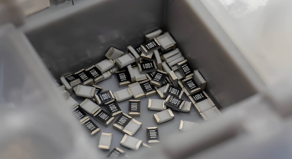
For chip resistors, capacitors, and inductors, package codes usually describe approximate dimensions in inches.
Package | Approximate Size | Practical Use |
0402 | 1.0 mm × 0.5 mm | High-density designs with controlled assembly |
0603 | 1.6 mm × 0.8 mm | A balanced option for many commercial products |
0805 | 2.0 mm × 1.25 mm | Easier manual inspection and rework |
1206 | 3.2 mm × 1.6 mm | Higher power or larger-value passive components |
Smaller packages save board space, but they do not automatically improve the product. A 0402 resistor may suit a dense wireless module, while a 0603 resistor can offer a more forgiving choice for prototypes, lower-volume builds, and field repair.
Choose the smallest package that supports the design requirements without creating unnecessary manufacturing risk. If the board does not need extreme density, a slightly larger package can improve placement tolerance, inspection visibility, and rework practicality.
3.2. Leaded IC Packages
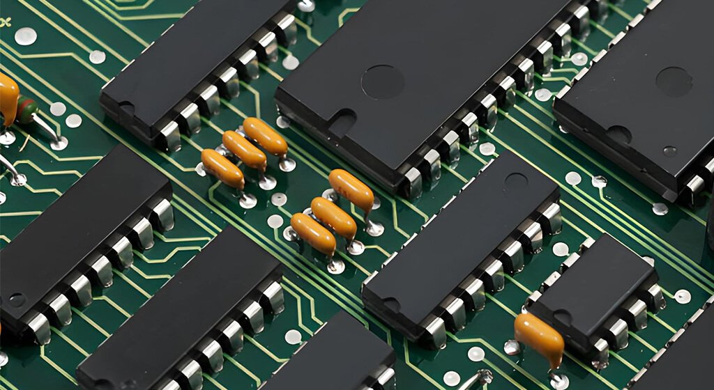
SOIC, SOP, TSSOP, and QFP packages use visible leads around the device body. Their solder joints are easier to inspect visually, and many can be reworked with conventional hot-air equipment.
These packages consume more board area than leadless alternatives. They can still be the right choice when serviceability, low-cost prototyping, or moderate pin counts matter more than maximum density.
3.3. Leadless Packages: QFN and DFN
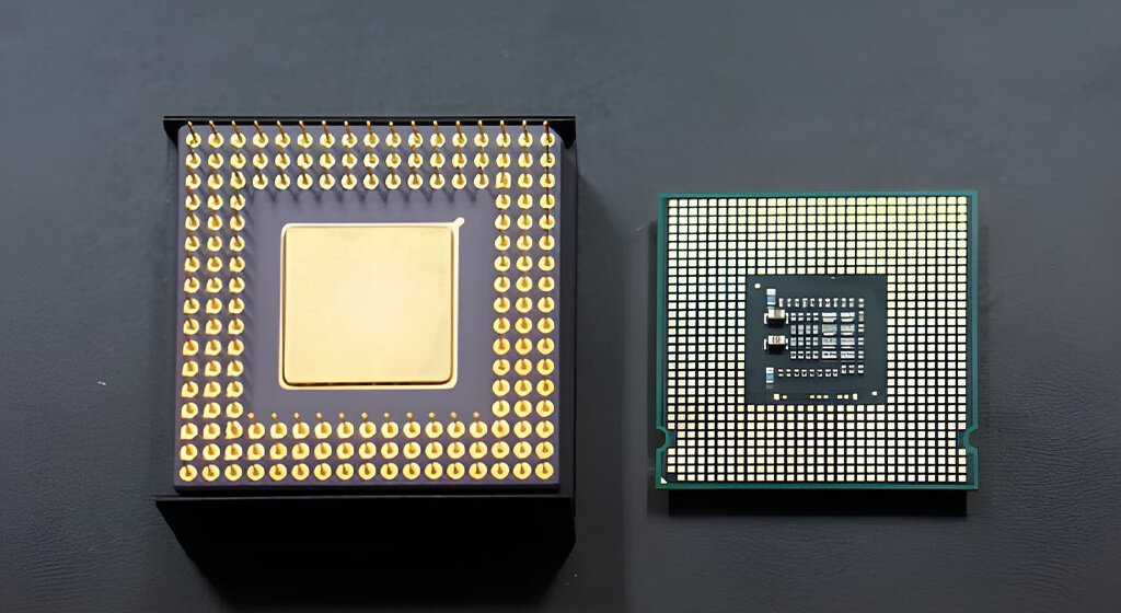
QFN and DFN packages reduce footprint size by placing contacts beneath the device body. They are common in RF circuits, power devices, wireless modules, and compact control boards.
Their compact shape can improve electrical performance by shortening interconnects. However, bottom-side terminals reduce direct visual access to some solder joints. The PCB land pattern, thermal pad design, stencil aperture, reflow profile, and inspection plan must work together.
3.4. BGA and Fine-Pitch Packages
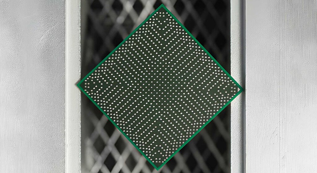
Ball Grid Array packages place solder balls underneath the device. They allow high pin counts within a relatively small footprint, making them common for processors, memory, and advanced communication devices.
BGA selection requires early planning. Routing fan-out, via strategy, board stack-up, assembly capability, X-ray inspection, rework access, and thermal design should be reviewed before finalizing the footprint.
IPC-7095E specifically addresses design and assembly implementation for BGA and fine-pitch BGA technology, with emphasis on inspection, rework, and reliability. That is a useful reminder that package selection should not be treated as a layout-only decision.
4. How to Select SMT Components for a New PCB?
A sensible selection process starts with circuit requirements, not with what happens to fit on the board.
4.1. Confirm Electrical Requirements First
Every part should meet the voltage, current, power, tolerance, frequency, and temperature requirements of the circuit. Those limits should come from the schematic and system requirements, rather than from a familiar component series.
A resistor’s value alone does not define its suitability. Its power rating, voltage rating, tolerance, temperature coefficient, pulse capability, and package all matter.
The same applies to capacitors. Check capacitance, voltage rating, dielectric type, temperature behavior, DC-bias effects, ESR, and expected lifetime.
For ICs, confirm the package, pinout, thermal-pad arrangement, firmware requirements, and product lifecycle before the BOM is released.
4.2. Verify Footprints and Land Patterns
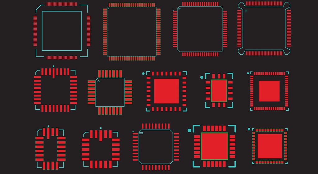
A component package must match the PCB footprint, the assembly process, and the inspection method. Do not assume that a CAD-library symbol is correct because it has been used before.
Always compare the footprint with the manufacturer’s current package drawing and recommended land pattern. Check pad size, solder-mask clearance, paste apertures, courtyard spacing, polarity marks, and pin-one orientation.
A footprint error can affect every board in the build. It may lead to placement problems, poor solder joints, difficult rework, or an expensive board revision.
4.3. Consider the Operating Environment
The component must survive the environment where the final product will operate. Temperature cycling, humidity, vibration, dust, chemicals, and electrical stress can change the selection decision.
A part that performs well in a desktop device may not suit an outdoor controller or industrial power unit. Automotive, medical, aerospace, and industrial projects may also require additional traceability, qualification, or customer-defined acceptance criteria.
4.4. Build Flexibility into the BOM
A strong BOM does not rely on one difficult-to-source part when qualified alternatives are available. During design review, identify components with limited distribution, long lead times, restricted availability, or an approaching end-of-life status.
For important components, identify approved alternatives that match the electrical requirements, package, pinout, firmware behavior, and qualification needs. A lower-cost substitute is not necessarily a compatible substitute.
NIST identifies counterfeits, unauthorized production, tampering, and poor manufacturing practices as supply-chain risks throughout a product lifecycle. That makes component provenance part of the engineering review, not just a purchasing task.
5. From BOM to Finished PCB Assembly
A smooth SMT build depends on clear information moving from design through sourcing and production. At a minimum, the manufacturing package should include Gerber files, a BOM, a pick-and-place file, an assembly drawing, revision information, and special process notes.
5.1. Choose the Right Sourcing Model
A full-turnkey build means the manufacturing partner manages PCB fabrication, component sourcing, assembly, testing, and delivery. This approach can simplify purchasing and reduce coordination between separate suppliers.
A partial-turnkey build means the customer supplies selected components, while the manufacturer sources the remainder. It can work well when an OEM holds proprietary ICs, allocated devices, or existing inventory.
A consigned build means the customer supplies all components. This provides more direct purchasing control, but it also requires careful management of quantities, labeling, packaging condition, and replacement materials.
PCBSAIL offers full and partial turnkey PCBA options for projects that need different sourcing models. The right choice depends on who can best manage supply risk and technical responsibility.
5.2. Review the BOM Before Purchasing
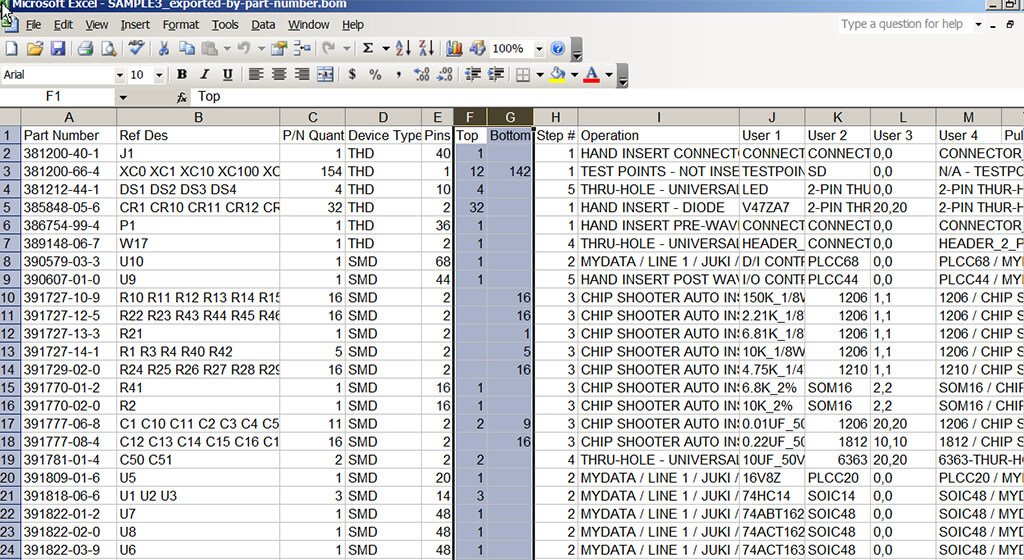
A BOM review should confirm manufacturer part numbers, packages, quantities, reference designators, approved alternatives, and lifecycle status. It should also flag parts that need programming, testing, special handling, or customer approval.
This review often catches problems before production begins:
- A BOM package does not match the PCB footprint.
- A polarity marking is unclear or inconsistent.
- A substitute uses a different pinout or exposed pad.
- A part is unavailable from an approved source.
- A programmed IC lacks a controlled firmware revision.
- A moisture-sensitive device has specific storage requirements.
PCBSAIL’s electronic component sourcing service covers part selection, alternative components, and sourcing considerations that are relevant during this stage.
5.3. Prepare for Placement and Reflow
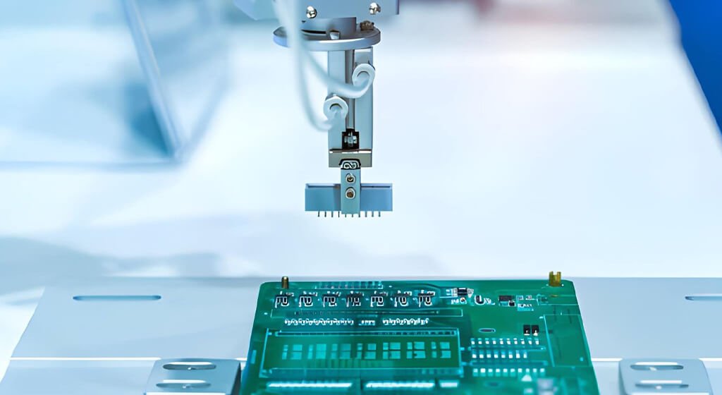
After the PCB and components are ready, solder paste is printed onto the pads through a stainless steel stencil. Automated placement equipment then positions each component using the pick-and-place data.
The populated board moves through a reflow oven, where the solder melts and forms the electrical and mechanical connection. Paste printing, placement, and reflow must be treated as connected processes.
A package with tight pitch, exposed pads, or uneven thermal mass may need a tailored stencil design and a controlled reflow profile. The wrong combination can lead to weak joints, bridging, voiding, or placement defects.
Moisture-sensitive devices require particular care. Infineon’s assembly guidance, based on JEDEC moisture-sensitivity classifications, lists a 168-hour floor life for MSL 3 components at up to 30°C and 60% relative humidity. The same document specifies baking before use for MSL 6 parts. The actual component label and manufacturer documentation should always take priority.
6. Common SMT Problems and How to Avoid Them

Many SMT defects are caused by a mismatch between the design, materials, machine setup, and process controls. The most effective prevention work happens before the first production panel enters the line.
Risk | Common Cause | Better Practice |
Tombstoning | Uneven heating or unbalanced pads | Use symmetrical pad geometry and balanced copper areas |
Solder Bridging | Excess paste, poor spacing, or misalignment | Review stencil apertures and component clearance |
Missing Or Shifted Parts | Incorrect centroid data or rotation settings | Verify reference designators, rotations, and fiducials |
Polarity Errors | Unclear markings or inconsistent library orientation | Standardize polarity marks and assembly drawings |
Open Solder Joints | Insufficient paste, contamination, or poor wetting | Check pad finish, paste deposits, and reflow settings |
BGA Defects | Hidden joints, warpage, or unsuitable process settings | Plan inspection and validation before production |
Inspection should reflect the package and the risk. Automated optical inspection can identify many visible problems, including missing parts, polarity errors, skew, and solder bridges.
X-ray inspection can help assess hidden joints beneath BGA and bottom-terminated packages. Electrical testing then confirms whether the completed board works as intended.
IPC separates soldering process requirements from final acceptance criteria. IPC J-STD-001 covers soldered assembly materials and process controls, while IPC-A-610 provides post-assembly acceptance criteria.
7. How Package Choices Affect Cost and Lead Time
The unit price of a component is only one part of the manufacturing cost. A low-cost part can create a more expensive build if it is hard to source, difficult to handle, or poorly suited to the assembly process.
Very small packages may require tighter placement tolerances, more demanding inspection, and specialized rework. Fine-pitch ICs can also affect routing density, stack-up requirements, and test access.
A BOM with too many unique part numbers can create unnecessary purchasing work. Standardizing values, packages, and approved component families often makes sourcing and production easier.
Lead time usually depends on the slowest part in the BOM. A technically sound board can still miss its production schedule when one critical part is obsolete, allocated, or only available through unverified channels.
Before releasing a BOM, ask:
- Is the part active and available from approved distributors?
- Is there a tested alternative with the same package and pinout?
- Does the package need special inspection or rework capability?
- Can the layout accommodate an approved replacement?
- Are lead-time assumptions based on current supplier information?
8. Compliance and Documentation

Compliance should be considered during component selection, not checked at the end of a project. For products placed on the EU market, the BOM and supplier declarations should support applicable RoHS requirements.
The EU RoHS Annex II lists ten restricted substances. Most have a maximum concentration value of 0.1% by weight in homogeneous materials, while cadmium has a maximum value of 0.01%. EU RoHS Directive 2015/863
A RoHS label does not automatically make a component suitable for every application. Buyers still need to check declarations, exemptions, customer requirements, and applicable regional regulations.
Documentation also protects future redesign work. A controlled BOM, approved alternate list, component library record, and assembly notes make it easier to manage changes without losing the original design intent.
9. Preparing for SMT Assembly
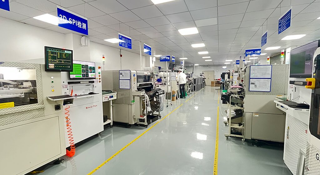
A capable manufacturing partner should be able to review the production package before assembly begins. The purpose is not simply to place components quickly. It is to build boards that can be sourced, assembled, inspected, tested, and repeated.
Our SMT assembly services cover DFM review, solder paste inspection, component placement, reflow, AOI, X-ray inspection, and electrical testing options.
Before requesting a quotation, prepare the latest Gerber files, BOM, centroid file, assembly drawing, approved alternatives, and any programming or test requirements. Clear documentation reduces delays and allows the engineering review to focus on genuine manufacturing risks.
10. Frequently Asked Questions About SMT Components
Are SMT Components And SMD Components The Same Thing?
Not exactly. SMT is the assembly method, while SMD refers to a component designed for surface mounting. However, “SMT components” is a common and widely understood industry search term.
Should I Choose 0402, 0603, Or 0805 Components?
Choose the smallest package that the design genuinely requires. For many products, 0603 offers a practical balance between density, availability, inspection, and rework.
Can SMT And Through-Hole Components Be Used On The Same PCB?
Yes. Mixed-technology boards are common. SMT provides density and automated placement, while through-hole parts can provide stronger mechanical mounting for connectors and heavy components.
Why Does Package Choice Matter When The Electrical Value Is Identical?
The package affects power handling, thermal performance, placement accuracy, PCB area, routing, inspection access, rework difficulty, and component availability. Two resistors with the same value can create very different production outcomes.
What Files Are Needed For An SMT Assembly Quotation?
Most manufacturers require Gerber files.
A BOM Include:
- Manufacturer part numbers
- Pick-and-place file
- Assembly drawing
- Special process instructions.
Programming files, test requirements, and approved alternatives should be included when relevant.
11. Request an SMT Component and Assembly Review
A dependable SMT build starts with a clear BOM and a manufacturable layout. Send your Gerber files, BOM, pick-and-place file, and assembly notes to PCBSAIL for a component-sourcing and manufacturability review.
Get a PCB Quote