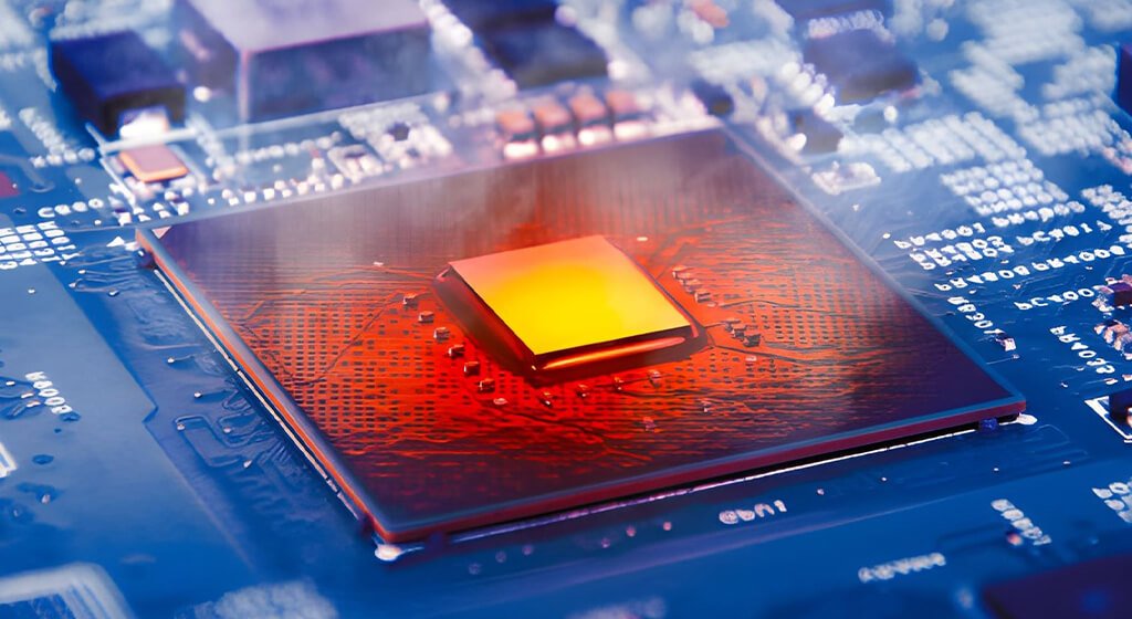
As devices become smaller, faster, and more powerful, PCB Thermal Management grows exponentially.
High-performance applications such as 5G base stations, AI, and EVs, generate substantial heat.
Without proper PCB thermal management, this heat can lead to performance throttling, device failures, reliability issues, and a drastically reduced lifespan of electronic systems.
Therefore, thermal management techniques for PCBs are now a fundamental part of the design process, not an afterthought.
This comprehensive guide explores advanced PCB thermal management techniques to help engineers implement effective thermal strategies.
Table of Contents
1. Why Is PCB Thermal Management Important?

Heat is unavoidable in electronic systems. Temperature Control PCBA, Power conversion circuits, processors, FPGAs, LEDs, MOSFETs, and voltage regulators all generate thermal energy.
If heat is not removed efficiently, several problems can occur:
- Reduced Component Lifespan
- Higher Failure Rates
- Signal Integrity Degradation
- Increased Power Losses
- Mechanical Stress From Thermal Cycling
As electronic products become smaller, thermal design is no longer optional. It is now a core engineering requirement.
2. How Does Heat Move Through a PCB?

Three mechanisms move heat inside electronic systems:
2.1. Conduction
Conduction is the primary heat transfer method in PCBs.
Heat Travels Through:
- Copper Traces
- Copper Planes
- Thermal Vias
- Metal Substrates
Copper conducts heat extremely well. Its thermal conductivity is approximately 385–390 W/m·K. FR-4 typically offers only 0.25–0.4 W/m·K.
That’s why thermal engineers rely heavily on copper structures.
2.2. Convection
Convection transfers heat from PCB surfaces to surrounding air.
Natural convection occurs without airflow.
Forced convection uses fans or blowers to increase heat removal.
Typical Convection Coefficients Range From
- 5–25 W/m²·K for natural cooling
- 25–100 W/m²·K for forced-air systems.
2.3. Radiation
Radiation contributes less heat removal than conduction or convection.
For most electronics operating below 125°C, radiation represents only a small portion of total heat dissipation.

Do You Need Any Help?
3.11 PCB Thermal Management Strategies
PCB thermal design is the cornerstone of effective heat management. The right decisions at the layout and material level significantly reduce operating temperatures and prevent reliability issues.
Below, we explore the most critical strategies.
3.1. Heat Spreading and Hot Spot Avoidance

High-power components, such as power transistors, regulators, and CPUs, generate localized heat.
Hot spots occur when heat generation exceeds local heat dissipation.
Common Causes Include:
- High-Power MOSFETS
- Voltage Regulators
- Processors
- FPGAS
- LEDs
- Power Resistors
To avoid hot spots, we recommend you distribute these components evenly across the PCB.
Use thermal zones, grouping heat-generating components together while keeping them physically separated from temperature-sensitive devices such as crystal oscillators, ADCs, and precision sensors.
3.2. Convection

Airflow can dramatically reduce PCB temperatures. Natural convection works in low-power systems. Forced-air cooling becomes necessary as power density increases.
Best Practices Include:
- Align Components With Airflow Direction
- Avoid Airflow Obstructions
- Create Dedicated Air Channels
- Position Fans Near Major Heat Sources
Practical Tip: Maintain a minimum spacing of 3–5 mm between high-power ICs to allow heat spreading and airflow.
Many thermal failures occur because airflow receives insufficient attention during enclosure design.
Even small airflow improvements can produce significant temperature reductions.
3.3. Copper Pours for Heat Spreading
Copper planes act as built-in heat spreaders. Because copper conducts heat roughly 1,000 times better than FR-4. Larger copper areas can distribute thermal energy across a wider surface.
Benefits Of Copper Planes Include:
- Lower Thermal Resistance
- Improved Temperature Uniformity
- Reduced Hot Spots
- Better Overall Reliability
Many engineers dedicate ground planes to both electrical and thermal functions. A continuous copper plane can dramatically improve heat spreading without increasing manufacturing complexity.
3.4. Increasing Copper Weight

Standard PCBs use 1 oz/ft² copper. For high-current or high-power applications, increasing to 2–3 oz/ft² significantly improves heat spreading.
Power electronics, such as EV inverters or LED modules, benefit greatly from thicker copper layers.
Copper Thickness | Thermal Conductivity Impact | Application Example |
1 oz/ft² | Standard | Consumer Electronics |
2 oz/ft² | Moderate Improvement | High-power Logic Boards |
3 oz/ft² | Significant Improvement | Power Converters, LED Drivers |
Design Tip: Combine copper pours with thermal vias for multi-layer heat dissipation.
3.5. Heat Transfer through Vias

Thermal vias are plated holes designed to conduct heat vertically through the PCB.
They Create A Direct Thermal Path Between:
- Top Copper Layers
- Internal Planes
- Bottom Copper Surfaces
The thermal conductivity of a via array can reach approximately 15–25 W/m·K. This is dramatically higher than FR-4 alone.
After we studied, a properly designed 5×5 thermal via array reduced thermal resistance by approximately 60%.
Key Design Guidelines Include:
- 0.3 mm Via Diameter
- 1.0–1.2 mm Pitch
- Dense Placement Beneath Thermal Pads
- Connection to Large Copper Planes
Thermal vias are most effective when combined with copper planes. A via without a heat-spreading plane delivers limited benefit.
Can Too Many Thermal Vias Be Used? The answer is yes.
Engineers often assume that more vias always improve cooling. However, thermal improvements eventually reach diminishing returns.
After a certain density, additional vias provide minimal temperature reduction.
Excessive Via Density Can Also:
- Increase Manufacturing Costs
- Create Drilling Challenges
- Reduce Mechanical Integrity
- Complicate Assembly
Successful thermal design focuses on optimization rather than maximizing via count.
Should Thermal Vias Be Connected to Pads? Most thermal vias should connect directly to thermal pads or copper pours associated with the heat source.
Without proper copper connections, heat transfer becomes inefficient. Many PCB designers use via-in-pad structures for high-power devices. Filled or capped vias help prevent solder wicking during assembly.
The exact approach depends on component requirements and manufacturing capabilities.
Do You Need Any Help?
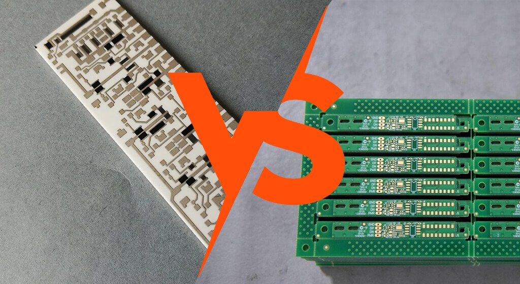
3.6. High Thermal Conductivity Materials

Material selection is crucial for effective PCB thermal management. Standard FR-4 boards have a thermal conductivity of ~0.3–0.4 W/mK, which is insufficient for high-power applications.
Alternatives Include:
Material | Thermal Conductivity | Applications |
0.3–0.4 W/mK | Standard PCBS | |
Metal Core PCB (Al) | 1.0–2.0 W/mK | High-Power LED, Automotive Power Modules |
3.0–4.0 W/mK | Extreme Power Electronics | |
20–200 W/mK | RF Devices, High-Reliability Aerospace Electronics |
Practical Tip: Use metal-core PCBs for LED lighting and power electronics to ensure uniform heat dissipation across the board.
3.7. Use Heat Sinks

Heatsinks become necessary when PCB-level techniques cannot maintain acceptable temperatures. A heatsink increases surface area and improves convection.
Common Heatsink Materials Include:
- Aluminum
- Copper
Thermal interface materials improve heat transfer between the component and heatsink.
These Include:
- Thermal Grease: Improves Surface Contact.
- Thermal Pads: Pre-Cut, Non-Curing Materials For Ease Of Assembly.
- Phase-Change Materials
Design Tip: Use finned heat sinks aligned with airflow paths to maximize convective cooling.
3.8. Use Fans and Forced Convection

Active airflow reduces boundary layer thermal resistance. We recommend you use fans with high static pressure for dense boards, ensuring heat is removed from hot zones efficiently.
Air channels or ducts can improve airflow over critical components, minimizing temperature gradients.
Practical Example: In high-end GPUs, fan and duct designs reduce die temperature by 15–20°C compared to passive cooling.
3.9. Heat Pipes & Vapor Chambers

Heat pipes and vapor chambers use phase change (liquid to vapor) to transfer heat rapidly. They are effective in confined spaces, such as laptops and compact embedded systems.
Advantages Include:
- High Thermal Efficiency
- Uniform Temperature Distribution
- Compact Implementation
Common Applications Include:
- Gaming Hardware
- Telecom Equipment
- Servers
- High-Performance Computing
Many modern electronics combine heat pipes with heatsinks and forced-air cooling.
3.10. Dielectric Fluid Immersion Cooling

PCBs are immersed in thermally conductive, electrically insulating fluids. Heat is transferred directly from the components to the fluid, which is then cooled via circulation or heat exchangers.
Applications:
- Data Centers
- 5G Base Stations
- High-Power Computing Modules
Advantages:
- Extremely Uniform Cooling
- Enables Higher Power Densities
- Reduces Reliance On Fans
Case Study: Google’s experimental immersion-cooled servers reduced operational temperatures by up to 25% while increasing system density.
3.11. Graphene Thermal Materials
Graphene is one of the most promising thermal materials under development.
Graphene exhibits thermal conductivity exceeding 2000 W/mK. It can be applied as films, pads, or coatings to improve PCB thermal performance.
Applications:
- Flexible Electronics
- High-performance RF Modules
- Wearable and IoT Devices
Future Potential: Graphene thermal interfaces promise ultra-thin, high-efficiency heat spreading solutions for compact PCBs, bridging the gap between passive and active cooling methods.
4. How Does PCB Stack-Up Affect Heat Dissipation?

PCB stack-up strongly influences thermal performance. Layer arrangement determines how heat spreads throughout the board.
Effective Thermal Stack-ups Often Include:
- Large Internal Ground Planes
- Continuous Power Planes
- Reduced Dielectric Thickness
- Heavy Copper Layers
Research shows that copper placement and dielectric structure significantly impact thermal resistance and heat flow paths.
Thermal planning should begin during stack-up definition, not after layout completion.
5. What Are the Most Common PCB Thermal Management Mistakes?
Engineers frequently encounter similar thermal design errors.
Common Mistakes Include:
- Ignoring Thermal Design Until Layout Completion.
- Using Insufficient Copper Area.
- Underestimating Airflow Requirements.
- Omitting Thermal Vias Beneath Power Devices.
- Placing Heat-Sensitive Components Near Hot Spots.
- Selecting Inappropriate Substrate Materials.
- Failing To Perform Thermal Simulation.
Most thermal problems originate during design rather than manufacturing. Preventive design is the most effective strategy.
6. Conclusion
PCB thermal management is no longer a secondary consideration. It is a fundamental requirement for modern electronics.
The most effective strategy combines multiple techniques. Component placement, copper planes, thermal vias, stack-up optimization, material selection, airflow management, and advanced cooling methods all contribute to thermal performance.
Among all techniques, thermal vias and copper planes is the most frequently discussed solutions because they deliver significant benefits with relatively low cost.
However, high-power applications increasingly require heatsinks, heat pipes, advanced substrates, and immersion cooling.
Engineers who prioritize thermal design early achieve lower operating temperatures, longer product life, improved reliability, and better overall system performance.
As electronic power density continues increasing, thermal management will be one of the most important disciplines in PCB engineering.
Get a PCB Quote