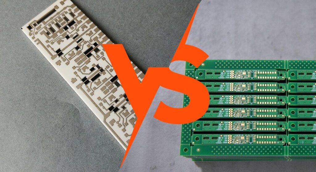
In today’s electronics-driven world, it is very important to find the right multi-Layer PCB manufacturer for your project. It can determine whether your product launches on time, performs reliably, and stays profitable.
As devices become smaller, faster, and more complex, businesses now need 4-layer, 6-layer, 8-layer, 10-layer, and high-layer PCBs with controlled impedance, fine traces, and thermal stability.
This guide will help you find a good multi-Layer PCB manufacturer for your project.
Table of Contents
1. What Is a Multi-Layer PCB?

A Multi-Layer PCB is a printed circuit board built with three or more conductive copper layers laminated together with insulating substrate materials under heat and pressure.
Unlike single-sided or double-sided PCBs, multilayer boards use internal copper layers for:
- Power Planes
- Ground Planes
- High-Speed Signal Routing
- Controlled Impedance Traces
- Dense Component Interconnections
Common Multilayer PCB Configurations Include:
- 4 Layer PCB
- 6 Layer PCB
- 8 Layer PCB
- 10 Layer PCB
- 12 Layer PCB
- 16+ Layer PCB
2. Why Multi-Layer PCB Demand Is Growing?
As industries move toward smarter, faster, and more compact devices, multilayer PCBs have become essential.
2.1. Electronics Are Becoming Smaller and More Powerful

Consumers and businesses expect devices that are:
- Thinner
- Lighter
- Faster
- More Feature-rich
To fit more components into the limited space, designers use Multi-Layer PCBs. It allows higher circuit density without increasing board size.
2.2. Rising Demand for High-Speed Data Transmission

Modern devices use high-speed communication standards such as:
- 5G
- Wi-Fi 7
- USB4
- PCIe
- DDR memory interfaces
These systems require excellent signal integrity, low noise, and controlled impedance. Multilayer PCBs provided dedicated signal, ground, and power planes that help maintain stable high-speed performance.
2.3. Better EMI Control and Reliability
Multilayer PCBs can reduce electromagnetic interference (EMI) through internal ground and shielding layers. They also improve durability because circuits are protected inside the board structure.
This Is Important For:
- Aerospace
- Telecom
- Defense
- Medical
- Industrial Systems

Do You Need Any Help?
3. How to Choose the Best Multi-Layer PCB Manufacturer?
It is important to select the right multi-Layer PCB manufacturer in electronics development. A strong supplier helps you launch faster, reduce risk, and scale production smoothly.
3.1. Verify Technical Capabilities First

Not every PCB factory can build complex multilayer boards consistently. Many suppliers can produce basic 4-layer boards, but fewer can reliably manufacture HDI, fine-pitch, impedance-controlled, or high-layer-count products.
Ask Whether The Manufacturer Supports:
- 4, 6, 8, 10+ Layer Boards
- Controlled Impedance
- Blind/Buried Vias
- Laser Microvias
- Fine Trace & Space Tolerances
- Backdrilling For High-Speed Boards
If your product is advanced, capability should be the first filter.
3.2. Check Quality Certifications

Reliable PCB suppliers usually maintain recognized certifications. These indicate structured process control and compliance.
Look For:
- ISO 9001
- UL Compliance
- RoHS Compliance
- IPC Standards Support
3.3. Review Their Inspection & Testing Process

Multi-Layer PCB quality depends heavily on process discipline. Good factories use multiple inspection stages, not only final visual checks.
Ask Whether They Use:
- AOI
- Electrical Continuity/Isolation Testing
- Flying Probe Test
- X-ray Inspection
- Microsection Analysis
- Impedance Verification
This is especially important for multilayer boards because many defects are internal and invisible.
3.4. Evaluate Engineering Support

The best manufacturers do more than “take files and ship boards.” They help prevent mistakes before production starts.
Strong engineering teams should offer:
- DFM Review
- Stackup Recommendations
- Material Selection Guidance
- Panelization Advice
- Cost Reduction Suggestions
- Yield Improvement Feedback
A supplier that catches design issues early can save thousands in respin costs.
3.5. Compare Lead Time and On-Time Delivery
A low price means little if delivery is late.
Ask For:
- Prototype Lead Time
- Standard Production Lead Time
- Rush Order Capability
- Shipping Methods For Your Country
For product launches, dependable scheduling often matters more than small price differences.
Do You Need Any Help?
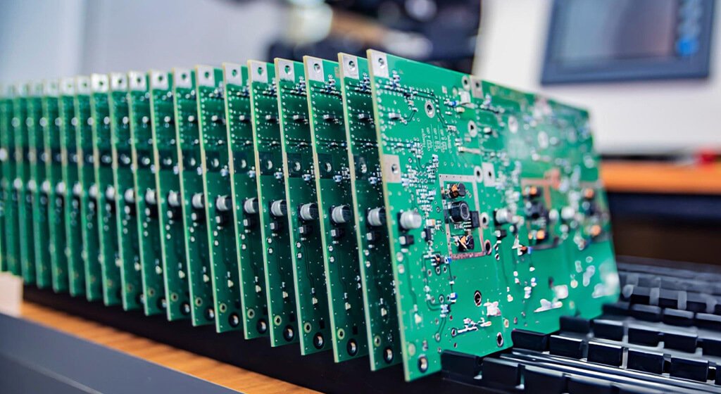
4. Top 10 Multi-Layer PCB Manufacturer To Recommend
Here’s a detailed overview of 10 reliable Multi-Layer PCB Manufacturers. These companies offer varying strengths in layer count, technology, turnaround time, quality standards, and geographic focus.
4.1. PCBSAIL

PCBSAIL is a professional full-service multilayer PCB manufacturer and PCBA provider capable of producing advanced multilayer boards from 4 to 64 layers. They specialize in complex stack-up planning, high-precision fabrication, and reliable lamination processes.
With ROHS & UL-certified quality systems and strong DFM support, PCBSAIL delivers high-reliability multilayer PCBs for demanding applications.
Their one-stop turnkey solution (design support, fabrication, component sourcing, and assembly) makes them an excellent choice for customers seeking cost-effective, scalable multilayer production with fast response times.
Aspect | Details |
Website | |
Featured Product | 4–64 Layer Multilayer PCB with Advanced Stackup |
Main Applications | Industrial control, automotive electronics, telecommunications, computing, medical devices, consumer electronics |
4.2. Philifast PCB

Philifast PCB is a fast-turnaround Chinese multilayer PCB manufacturer offering reliable multilayer fabrication and full turnkey PCBA services. They support complex multilayer designs with precise lamination and assembly capabilities.
Known for speed from prototype to mass production, Philifast serves a wide range of industries requiring high-density interconnects and consistent quality at competitive prices.
Aspect | Details |
Website | |
Featured Product | High-Precision Multilayer PCB + Turnkey PCBA |
Main Applications | Consumer electronics, automotive systems, medical devices, LED lighting, industrial control, smart home |
4.3. JLJ PCB

JLJ focuses on precision multilayer PCB manufacturing with emphasis on tight tolerances and reliable performance. They provide quality multilayer solutions suitable for mid-to-high complexity designs.
JLJ is recognized as a dependable option for customers needing consistent multilayer fabrication and technical accuracy in electronics production.
Aspect | Details |
Website | https://jlcpcb.com/ |
Featured Product | Precision Multilayer PCB |
Main Applications | Industrial electronics, control systems, general multilayer applications |
4.4. Sierra Assembly

Sierra Assembly is a trusted U.S.-based multilayer PCB manufacturer with extensive experience in multilayer fabrication and assembly.
They produce high-quality multilayer boards using advanced equipment while maintaining strict quality and compliance standards (RoHS & ISO). Sierra excels in turning complex multilayer designs into reliable, production-ready solutions with fast delivery and strong engineering support.
Aspect | Details |
Website | |
Featured Product | High-Quality Multilayer PCB Fabrication & Assembly |
Main Applications | Industrial, commercial electronics, automotive, medical devices |
4.5. Cirexx International, Inc

Cirexx International is a U.S.-based specialist with over 40 years of experience in complex PCB manufacturing. They are experts in multilayer, rigid-flex, and HDI multilayer boards, offering complete in-house layout, fabrication, and assembly services.
Cirexx is particularly strong in high-reliability and specialty material multilayer projects for advanced technology sectors.
Aspect | Details |
Website | |
Featured Product | Complex Multilayer & Rigid-Flex PCBs |
Main Applications | Aerospace, defense, medical, RF/microwave, high-reliability electronics |
Do You Need Any Help?
4.6. AdvancedPCB

AdvancedPCB is a leading U.S. multilayer PCB manufacturer known for advanced manufacturing capabilities.
They offer a wide range of laminate materials (FR-4, halogen-free, high-Tg, etc.) and support complex designs with excellent quality control.
AdvancedPCB is favored for its reliability, fast turnaround options, and technical expertise in high-performance multilayer applications.
Aspect | Details |
Website | |
Featured Product | Advanced Multilayer PCB up to 40 Layers |
Main Applications | Telecommunications, computing, aerospace, industrial, high-speed electronics |
4.7. Multi Circuit Boards

Multi Circuit Boards is a European supplier specializing in high-tech multilayer PCBs up to 48 layers. They provide quick online quoting, advanced options like blind/buried vias, impedance control, and back-drilling.
Known for high quality combined with competitive pricing and fast production (from 1 working day), they serve customers across Europe needing complex multilayer solutions.
Aspect | Details |
Website | |
Featured Product | High-Tech Multilayer PCB up to 48 Layers |
Main Applications | Industrial electronics, telecommunications, medical, high-density HDI designs |
4.8. Ucreate Electronic Group

Ucreate Electronic Group is a professional Chinese multilayer PCB manufacturer offering one-stop PCB and PCBA services.
With over 20 years of experience, they produce reliable multilayer rigid, flex, and rigid-flex boards. Ucreate emphasizes quality testing, impedance control, and full turnkey solutions, making them a strong partner for cost-effective multilayer production across various industries.
Aspect | Details |
Website | |
Featured Product | One-Stop Multilayer PCB & PCBA |
Main Applications | Consumer electronics, automotive, industrial control, medical, communication devices |
4.9. NCAB Group

NCAB Group is a global PCB supplier and one of the leading players in the multilayer PCB segment.
They source and deliver high-quality multilayer boards through a carefully selected factory network, with strict quality specifications that often exceed IPC standards.
NCAB excels in complex multilayer, HDI, and RF multilayer solutions with strong technical support and consistent global delivery.
Aspect | Details |
Website | |
Featured Product | High-Reliability Multilayer & HDI PCBs |
Main Applications | Industrial, automotive, telecom, medical, defense, high-performance electronics |
4.10. Rush PCB

Rush PCB is a well-established U.S.-based multilayer PCB manufacturer specializing in high layer count and complex multilayer boards.
They are known for advanced capabilities such as laser-drilled micro-vias, blind/buried vias, and high-reliability production.
Rush PCB offers full turnkey services and is a preferred partner for customers requiring premium quality multilayer PCBs in North America.
Aspect | Details |
Website | |
Featured Product | High Layer Count Multilayer & HDI PCBs |
Main Applications | Aerospace, defense, medical, telecommunications, industrial electronics |
Do You Need Any Help?
5. What Is Multi-Layer PCB Problems and How Good Manufacturers Prevent Them?
Because Multi-Layer PCB involve multiple laminated copper and dielectric layers, they are more complex to manufacture than 2-layer boards.
Without tight process control, Multi-Layer PCBs can suffer from internal defects, reliability failures, and assembly issues. That is why choosing an experienced manufacturer matters.
Below are the most common multilayer PCB problems and how good manufacturers prevent them.
- Delamination
- Misregistration (Layer Alignment Error)
- Via Failure
- Open Circuits and Short Circuits
- Impedance Out of Tolerance
- Warpage and Bow/Twist
- Solder Mask Misalignment
Next, we will further explore them.
5.1. Delamination

Delamination happens when the internal layers separate from each other after fabrication or during operation. This weakens the board and can cause electrical failure.
Common Causes
- Poor lamination pressure or temperature control
- Moisture absorbed in materials
- Low-quality prepreg or laminate
- Excessive thermal stress during soldering
How Good Manufacturers Prevent It
- Use premium laminate materials
- Bake materials before lamination
- Control press temperature, pressure, and dwell time
- Run thermal shock testing
- Maintain moisture-controlled storage
5.2. Misregistration (Layer Alignment Error)

Inner layers are not perfectly aligned, causing pad shift, annular ring reduction, or open circuits.
Common Causes
- Poor tooling accuracy
- Material movement during lamination
- Weak optical alignment process
How Good Manufacturers Prevent It
- CCD optical registration systems
- X-ray layer alignment checks
- Tight dimensional compensation controls
- Stable lamination cycles
5.3. Via Failure
Vias crack, open, or lose conductivity after thermal cycling.
Common Causes
- Thin copper plating inside holes
- Poor desmear process
- Incorrect aspect ratio design
- Expansion mismatch during heating
How Good Manufacturers Prevent It
- Adequate hole wall copper thickness
- Plasma/desmear optimization
- IPC-compliant via design rules
- Thermal cycling reliability tests
- Microsection inspection
5.4. Open Circuits and Short Circuits

Broken traces create opens, while copper bridging creates shorts.
Common Causes
- Etching defects
- Imaging errors
- Copper residue
- Dust contamination
How Good Manufacturers Prevent It
- Cleanroom imaging areas
- AOI (Automated Optical Inspection)
- Controlled etching chemistry
- Electrical continuity testing on every board
5.5. Impedance Out of Tolerance

Trace impedance does not match design requirements, causing signal loss or instability.
Common Causes
- Incorrect dielectric thickness
- Trace width variation
- Material inconsistency
- Poor stackup control
How Good Manufacturers Prevent It
- Controlled impedance stackup engineering
- TDR impedance testing
- Tight trace width process control
- Use stable dielectric materials
Do You Need Any Help?
5.6. Warpage and Bow/Twist

Board bends or twists, causing assembly problems and poor solder joints.
Common Causes
- Uneven copper distribution
- Incorrect cooling after lamination
- Poor material balance
- Thin board with many layers
How Good Manufacturers Prevent It
- Balanced copper design review
- Controlled cooling cycles
- Material symmetry in stackup
- Flatness inspection before shipment
5.7. Solder Mask Misalignment

Mask openings shift, exposing copper or covering pads.
Common Causes
- Registration drift
- Poor artwork alignment
- Expansion during curing
How Good Manufacturers Prevent It
- LDI (Laser Direct Imaging) for mask application
- Registration compensation software
- Final visual inspection
Do You Need Any Help?
6. Why PCBSAIL Is a Strong Choice for Multi-Layer PCB Projects?
PCBSAIL can be a strong choice when you need a balance of cost efficiency, engineering support, scalable production, and responsive service.
6.1. Strong Fit for Prototype to Production Projects

PCBSAIL is positioned well for customers needing:
- Early-stage prototypes
- Engineering validation builds
- Pilot production runs
- Full-scale mass production
- Ongoing repeat orders
It makes it useful for startups, OEM brands, and industrial equipment makers.
6.2. Multilayer PCB Capability Matches Modern Demand

Modern electronics increasingly require multilayer designs for density, signal quality, and compact packaging.
We Can Do:
Item | Capability |
Layer Count | 4–64 Layers |
Base Materials | FR-4 Tg 150–180 °C /Megtron /Rogers /Isola low-loss |
Board Thickness | 0.6–8.0 mm |
Copper Weight | 0.5–4 oz |
Min Trace/Space | 25/25 μm |
Min Hole Size | 0.05 mm (two mil) |
Via Technology | Through-hole/blind/buried/ Microvias/ stacked vias/via-in-pad |
Max Panel Size | 571.5 × 1200 mm |
Impedance Control | ±5% (plus/minus five percent) |
Surface Finish | ENIG, OSP, Immersion Silver |
Quality Testing | 100% E-test, AOI, X-ray, microsection |
Certifications | ISO 9001, UL, RoHS/REACH |
Lead Time | 5–7 days (five to seven) |
6.3. Engineering Support
We can do more than manufacture files—we help improve manufacturability.
Useful Support Includes:
- DFM review
- Stackup suggestions
- Material recommendations
- Panelization optimization
- Yield-risk warnings
- Cost-down recommendations
Our Strong engineering involvement can prevent respins and delays.
Do You Need Any Help?
7. How Multi-Layer PCBs Are Manufactured in PCBSAIL?
At PCBSAIL, multilayer PCB manufacturing follows a controlled process, which deliver reliable layer bonding, accurate registration, stable impedance, and consistent electrical performance.
7.1. Engineering File Review

Before production begins, our engineering team reviews customer data to ensure the design is manufacturable.
Typical Checks Include:
- Gerber files
- Drill files
- Layer count
- Board thickness
- Copper weight
- Trace/space tolerance
- Via sizes
- Controlled impedance requirements
- Surface finish selection
- Panelization efficiency
This stage helps reduce delays and prevent costly errors.
7.2. Material Preparation

We will select raw materials based on project requirements.
Common Material Options Include:
- Standard FR4
- High Tg FR4
- Low-loss materials
- High-frequency laminates
- Heavy copper cores (if needed)
Materials are inspected before use to ensure consistency in thickness, resin quality, and copper foil condition.
7.3. Inner Layer Imaging

We can do more than manufacture files—we help improve manufacturability.
Useful Support Includes:
- DFM review
- Stackup suggestions
- Material recommendations
- Panelization optimization
- Yield-risk warnings
- Cost-down recommendations
Our Strong engineering involvement can prevent respins and delays.
7.4. Inner Layer AOI Inspection

Each inner layer is checked using Automated Optical Inspection (AOI).
AOI Detects:
- Opens
- Shorts
- Missing Copper
- Over-etching
- Under-etching
- Fine-line defects
Finding defects before lamination is critical because internal layers cannot be repaired easily afterward.
7.5. Oxide / Surface Treatment

Before pressing layers together, inner copper surfaces are chemically treated to improve bonding between copper and prepreg resin.
It Improves:
- Lamination strength
- Thermal Reliability
- Resistance to Delamination
Do You Need Any Help?
7.6. Layer Stackup and Lamination

This is the core process of multilayer PCB manufacturing.
PCBSAIL Stacks:
- Inner layer cores
- Prepreg sheets
- Copper foil outer layers
Then the stack enters a lamination press using controlled:
- Heat
- Pressure
- Vacuum
- Time cycles
The result is a solid multilayer board panel with permanently bonded internal layers.
For high-layer-count or HDI boards, multiple lamination cycles may be required.
7.7. Drilling

After lamination, holes are drilled for vias and component leads.
Methods Include:
- Mechanical drilling for standard holes
- Laser drilling for microvias (HDI boards)
Hole accuracy is essential for registration and electrical reliability.
7.8. Hole Wall Metallization / Copper Plating

Drilled holes are made conductive through chemical copper deposition followed by electrolytic copper plating.
This creates electrical connection between layers.
Good Plating Ensures:
- Via reliability
- Thermal cycling durability
- Low resistance interconnects
7.9. Outer Layer Imaging and Etching

Once vias are plated, top and bottom copper layers are patterned.
Steps:
- Apply photoresist
- Image circuit pattern
- Copper plate pattern areas
- Tin protect circuit
- Etch unwanted copper
- Strip temporary coating
This creates the final external circuitry.
7.10. Solder Mask Application

Protective solder mask is applied to prevent oxidation and solder bridging.
Common Colors:
- Green
- Black
- Blue
- Red
- White
PCBSAIL may use LDI solder mask imaging for higher precision.
7.11. Surface Finish

Pads receive final finish for solderability and shelf life.
Common Options:
- HASL
- Lead-free HASL
- ENIG
- OSP
- Immersion Tin
- Immersion Silver
Choice depends on assembly method, pitch, and budget.
7.12. Silkscreen Printing

Legend printing adds:
Component References
- Logos
- Polarity marks
- Date codes
- Part numbers
7.13. Routing / V-Cut / Profiling

Boards are separated from production panels using:
- CNC routing
- V-scoring
- Punching (special cases)
This defines final board dimensions.
7.14. Electrical Testing

Every multilayer PCB should undergo electrical verification.
Tests Include:
- Continuity
- Isolation
- Netlist matching
Common Methods:
- Flying probe test
- Fixture test (for volume orders)
7.15. Final Quality Inspection
PCBSAIL final QC may check:
- Hole quality
- Surface finish
- Solder mask registration
- Silkscreen clarity
- Board thickness
- Dimension tolerance
- Warpage
- Packaging condition
7.16. Packaging and Shipment

Boards are vacuum sealed or moisture protected, then packed for export.
Packaging Often Includes:
- Vacuum bags
- Desiccant
- ESD-safe handling
- Carton protection
Do You Need Any Help?
8. How to Reduce Multilayer PCB Cost In PCBSAIL?
Because multilayer boards involve more lamination cycles, drilling, plating, materials, and inspection than 2-layer boards, every design choice affects price.
For buyers working with PCBSAIL, cost can often be lowered significantly through smart engineering and purchasing decisions.
8.1. Use the Lowest Practical Layer Count
Layer count is one of the biggest cost drivers.
Before ordering, ask whether your design truly needs extra routing layers or if optimization can reduce the stackup.
Cost Saving Tip:
Many designs can move from 8 layers to 6 layers with better routing strategy.
8.2. Standardize Board Thickness
Non-standard thicknesses can increase setup cost and material sourcing complexity.
Lower-cost Common Thicknesses Include:
- 1.0 mm
- 1.2 mm
- 1.6 mm
- 2.0 mm
8.3. Choose Standard Materials Unless Performance Requires More
Standard FR4 is usually the most economical option.
Premium Materials Cost More:
- Rogers
- PTFE
- Ceramic
- Low-loss high-speed laminates
- High Tg specialty grades
8.4. Optimize Board Size
PCB cost is heavily influenced by panel utilization.
Larger boards = fewer units per panel = higher unit cost.
Cost Saving Tip
Even small reductions in PCB outline dimensions can significantly improve panel efficiency.
Ask PCBSAIL to Review:
- Better dimensions
- Rotated panel layout
- Shared rails
- Tighter spacing (if manufacturable)
8.5. Avoid Unnecessarily Tight Trace/Space Rules
Very fine features increase yield risk and process difficulty.
Examples:
- 4/4 mil costs more than 6/6 mil
- 3/3 mil costs much more than standard rules
Use standard design rules whenever possible.
Do You Need Any Help?
8.6. Minimize Blind / Buried Vias
Blind vias, buried vias, and HDI microvias can raise cost sharply because they often require:
- Laser drilling
- Sequential lamination
- Additional process steps
If through-hole vias can achieve the same result, they are usually cheaper.
9. People Also Ask?
What Is The Most Common Multilayer PCB?
4-layer PCB is the most common for commercial products.
How Long Does Manufacturing Take?
Typical Lead Times:
- Prototype: 24 hours to 7 days
- Production: 2 to 4 weeks depending on complexity
Is Multilayer PCB Expensive?
More expensive than 2-layer boards, but often cheaper overall because it reduces product size and improves performance.
What Files Are Needed?
Usually:
- Gerber files
- Drill files
- Readme notes
- BOM (for assembly)
10. Final Thoughts
In 2026, successful electronics brands need a partner who can deliver engineering support, stable quality, fast turnaround, and scalable production.
Whether you need 4-layer prototypes or 8-layer networking boards, the right manufacturer reduces delays, lowers risk, and improves product reliability.
If you are looking for a dependable supplier, PCBSAIL can support your next project from prototype to mass production.
Get a PCB Quote