PCB Pad Design: Types, Guidelines, Defects, and DFM Checklist
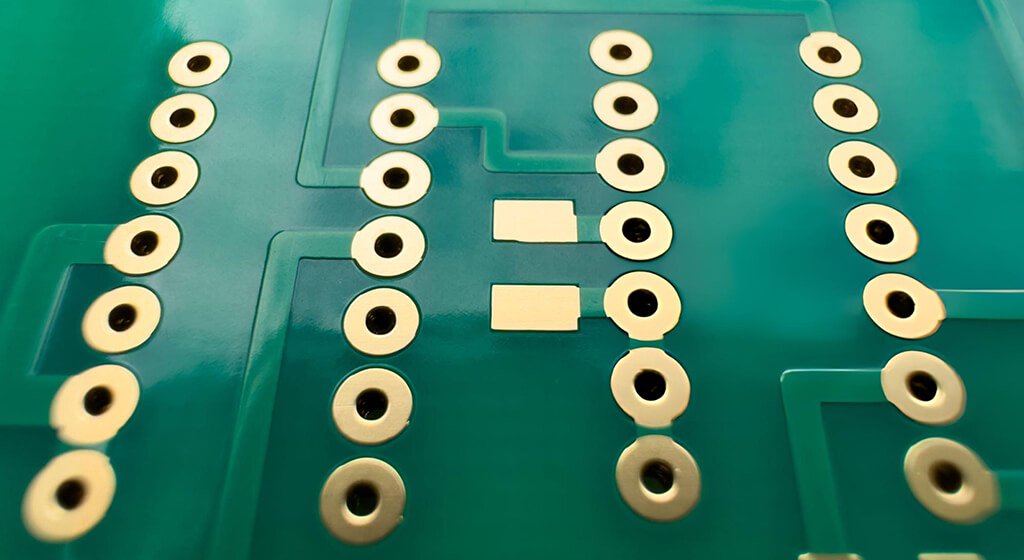
A PCB pad is an exposed conductive area used to solder, connect, test, or thermally couple a component to a printed circuit board. Its final

A PCB pad is an exposed conductive area used to solder, connect, test, or thermally couple a component to a printed circuit board. Its final
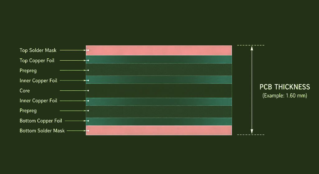
PCB thickness is the distance between the two outer faces of a manufactured printed circuit board. A rigid FR-4 PCB often starts at a nominal
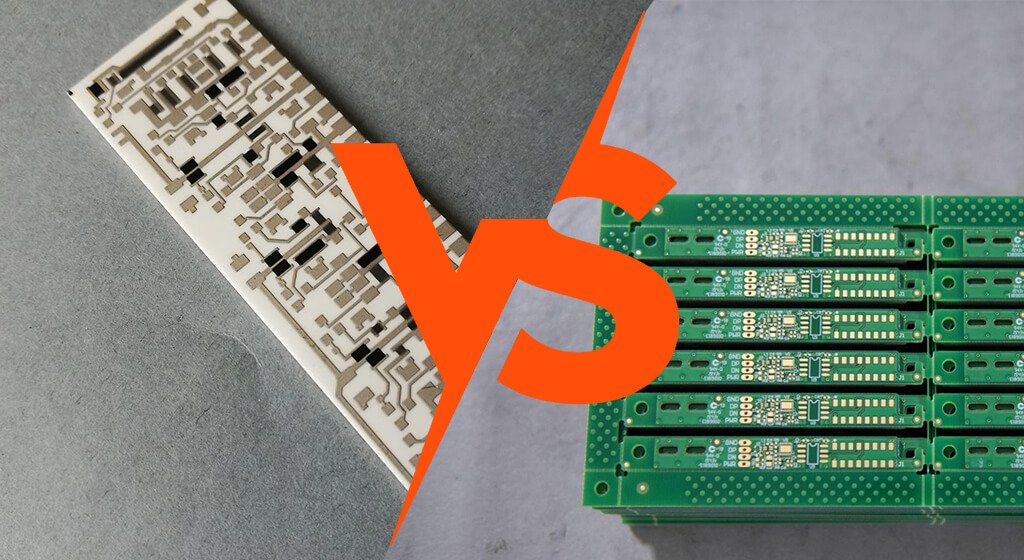
Ceramic PCB and FR4 are main substrate on market. FR4 is the standard substrate for most commercial electronics because it is affordable, scalable, and easy
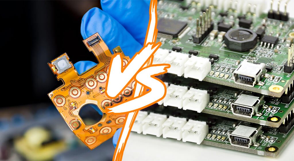
In PCB manufacturing, PCB material is one of the most important factors in electronics design. The material affects thermal performance, reliability, signal integrity, manufacturing cost,
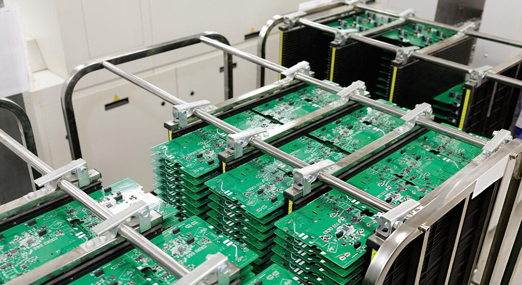
A good PCB assembly supplier is very important to your electronics project. It is not a simple sourcing decision. It directly affects product reliability, time-to-market,
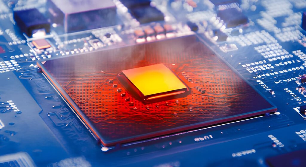
As devices become smaller, faster, and more powerful, PCB Thermal Management grows exponentially. High-performance applications such as 5G base stations, AI, and EVs, generate substantial
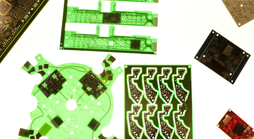
The global flexible electronics market grows rapidly. Multiple industry reports estimate the market could exceed $50 billion before 2030. Flexible printed circuit boards are now
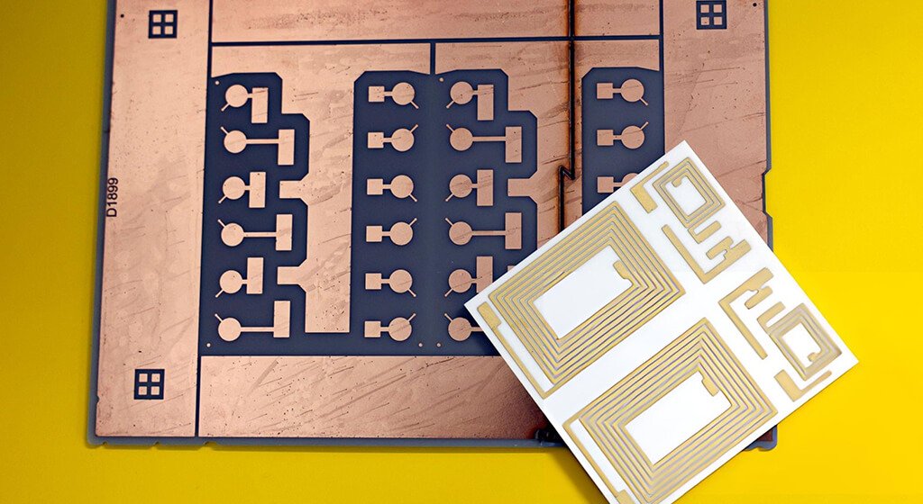
Ceramic PCBs have become essential in high-power electronics, EV systems, and RF applications. Traditional FR4 often fails under extreme heat, high current density, or aggressive
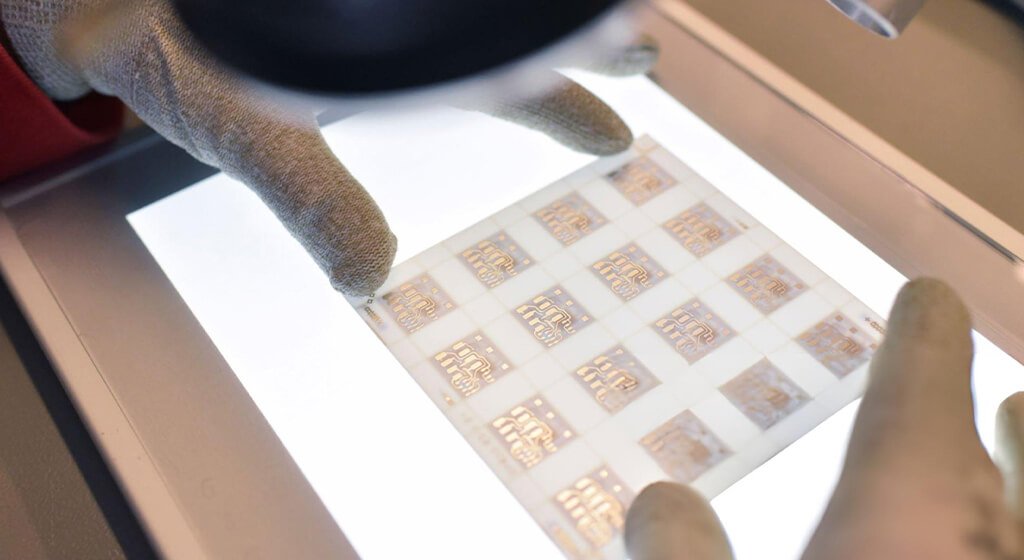
Ceramic PCB is rapidly becoming important in industries where FR4 boards can no longer meet thermal, electrical, or reliability requirements. From EV power modules to