
/From Prototype To Massive Production/

Fine Pitch SMT Assembly

PCBSAIL can offer fine pitch PCB assemblies with 0201 passives, QFN, DFN, QFP, CSP, LGA, BGA and micro BGA packages. Our SMT capability reaches 0.3 mm pitch, subject to package and design review.

Each build can combine PCB fabrication, component sourcing, 3D solder paste inspection, automated optical inspection, X-ray inspection and product-specific testing.

Min. Leaded-Component Pitch: 0.3 Mm

Min. Passive Package: 0201

Years of Experience
+ 0
On-Time Delivery
0 %

What Is Fine Pitch SMT Assembly?

Fine Pitch SMT Assembly is a surface mount technology (SMT) manufacturing process. It placed and soldered electronic components with very small lead spacing, pad sizes, and package dimensions onto a PCB.

Fine pitch assembly is commonly used in high-density electronic products such as medical devices, automotive electronics, industrial controls, telecommunications equipment, smartphones, aerospace systems, and IoT products.

Components and Packages We Assemble

We can offer several fine-pitch package families.

Fine Pitch SMT Assembly 0201 Passives

0201 Passives

An 0201 resistor or capacitor leaves little room for paste offset. Unequal deposits, mismatched pad geometry or uneven heating can pull the part upright or sideways during reflow. We uses supported panels, controlled printing, placement vision and AOI to manage these risks.
Fine Pitch SMT Assembly Fine-Pitch QFP and TQFP

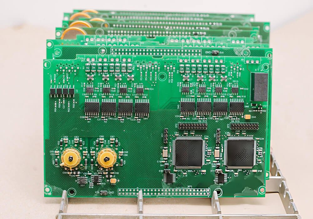
Fine-Pitch QFP and TQFP

Gull-wing leads make solder bridging and bent leads visible, but the narrow spacing increases sensitivity to stencil alignment and paste volume. Local fiducials can improve correction near a large, fine-pitch package.
Fine Pitch SMT Assembly QFN and DFN

QFN and DFN

QFN and DFN packages combine perimeter terminations with a center thermal pad. A segmented stencil aperture helps control the deposit and gives flux volatiles a path to escape.
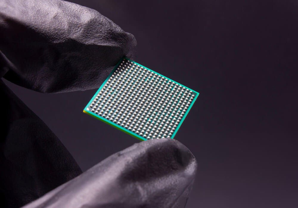
Fine Pitch SMT Assembly CSP, LGA, BGA and Micro BGA

CSP, LGA, BGA and Micro BGA

Area-array packages hide their joints beneath the body. Pad definition, via construction, moisture exposure, package warpage and reflow conditions all influence the result. We will review pad design, via-in-pad, stencil design and assembly.
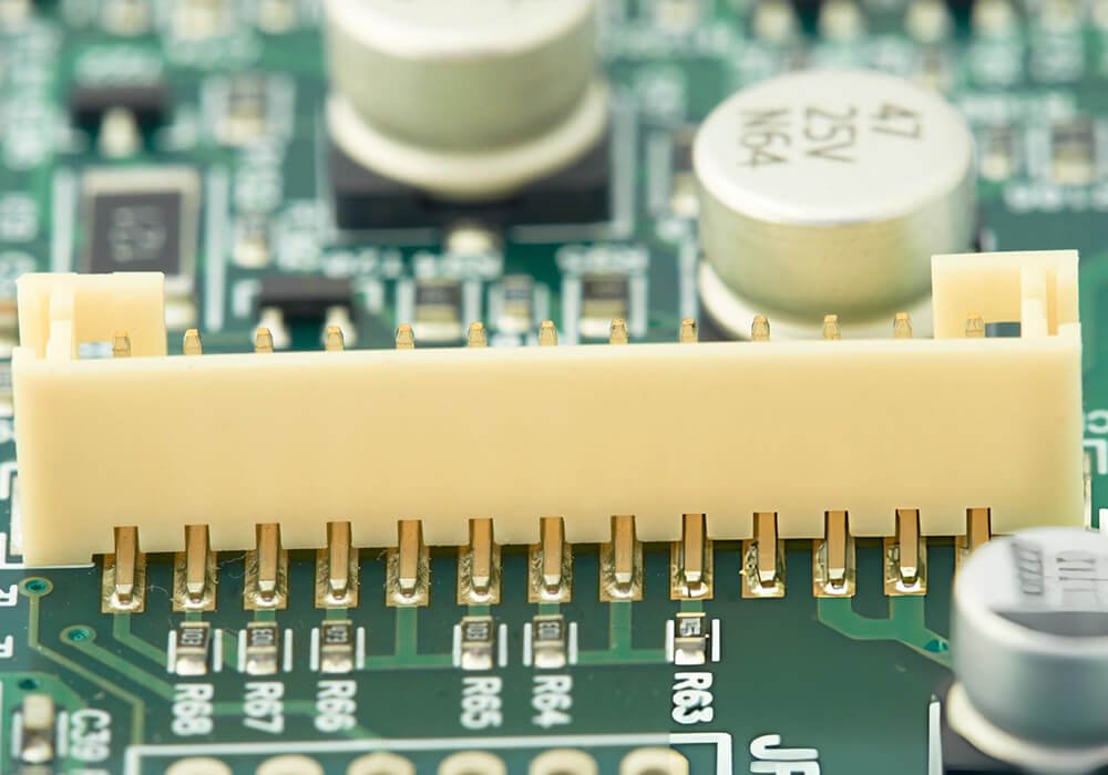
Fine Pitch SMT Assembly Fine-Pitch Connectors

Fine-Pitch Connectors

Long board-to-board or flex connectors can amplify local placement and coplanarity errors across a row of contacts. Stable board support, suitable local fiducials and verified paste deposits help control the joint pattern.
Fine Pitch SMT Assembly Capabilities

We can offer 0.3 mm min. pitch for leaded parts and BGA packages and 0201 smallest chip component. Our placement accuracy can reach 25 μm.

Capability

Specification

Min. Leaded-Component Pitch

0.3 mm pitch for fine-pitch leaded devices

Min. BGA Pitch

0.3 mm BGA pitch

Smallest Passive Components

Supports 0201 passive components

Fine-Pitch Package 

QFP, QFN, DFN, CSP, LGA, BGA, micro BGA, and fine-pitch connectors

Assembly Configuration

SMT, and mixed technology assembly (SMT + through-hole)

Solder Paste Verification

3D Solder Paste Inspection

Visible Solder Joint Inspection

Automated Optical Inspection

Hidden Solder Joint Inspection

X-ray inspection

Electrical Verification

ICT, functional testing, flying probe testing

Component Sourcing Model

Turnkey sourcing, customer-supplied materials (consigned), or hybrid supply model

What Should You Send?

How We Control the Fine-Pitch Process

We control fine-pitch assembly as a linked sequence rather than a placement-only task.

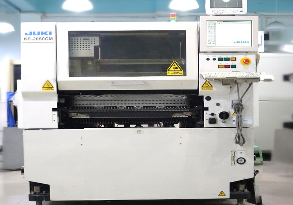
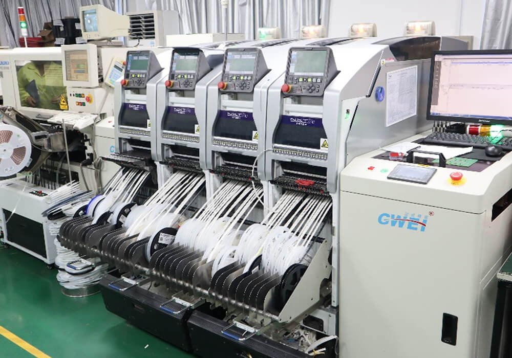
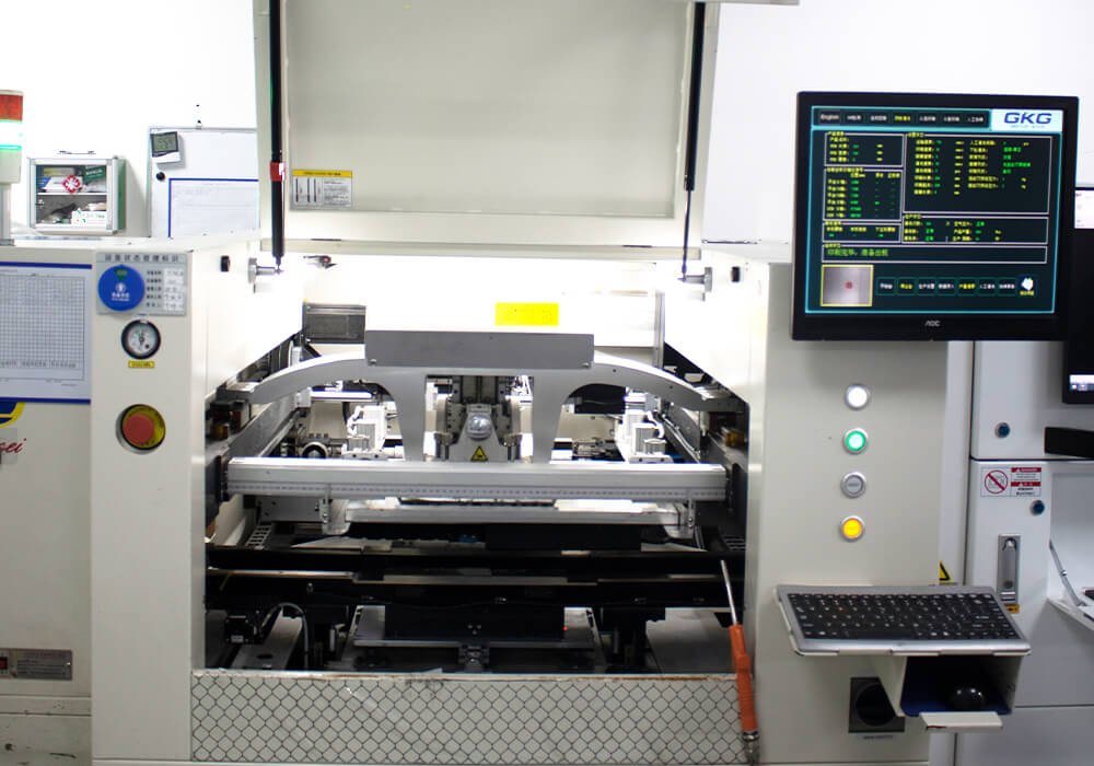
SMT Assembly Equipment

1. Data and DFM Review

Our engineers review the fabrication data, BOM, placement file, assembly drawings and quality requirements.

2. PCB and Land-Pattern Review

The bare board must support the intended assembly route. We will review pad size, mask registration, mask dams, surface finish, via-in-pad, copper balance and panel stiffness.

3. Stencil Engineering and Paste Printing

Stencil thickness and aperture geometry determine the initial solder volume. Boards that mix 0201 parts, fine-pitch ICs and large power components may need local aperture changes or a stepped stencil.

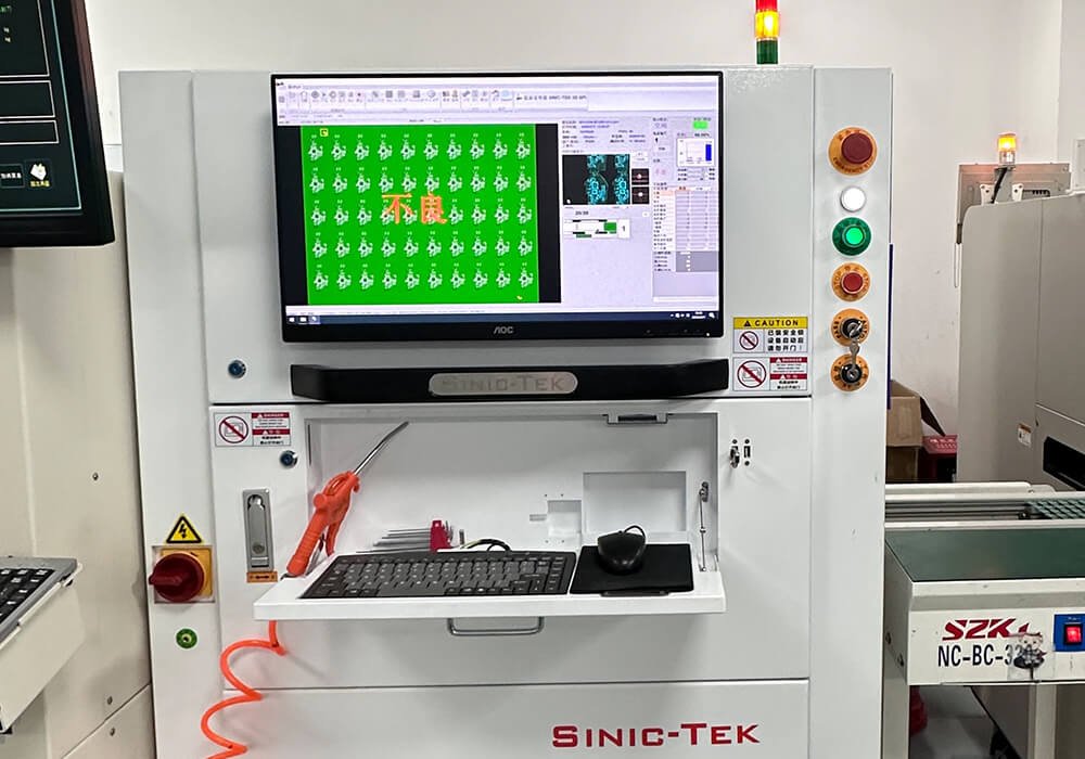
4. 3D Solder Paste Inspection

SPI checks deposits before components cover the pads. It can detect missing paste, low or excessive volume, offset and irregular deposits.

5. Vision-Guided Placement and First Article

The placement system uses component recognition and PCB fiducials to correct position and rotation.

6. Profiled Reflow

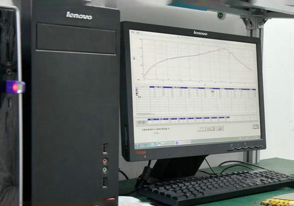
The reflow profile must suit the solder paste, board construction and component temperature limits. We profile the assembly route.

7. Inspection and Electrical Verification

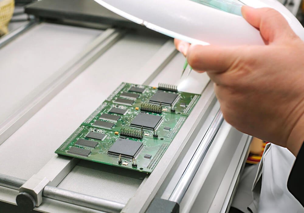
AOI checks visible placement and solder features. X-ray examines joints hidden under QFN, CSP, LGA and BGA bodies. ICT, flying-probe or functional testing can check electrical behavior when test access and customer data permit.

Why Choose Us for Fine Pitch PCBA??

Our team can coordinate sourcing, stencil planning, assembly, inspection, testing and shipment from prototype through repeat production. In our factroy, the PCB and assembly files can be reviewed together.

SPI, AOI and X-ray address different defect classes.

SMT, through-hole and mixed assemblies.

Turnkey, consigned and hybrid sourcing models are available.

Inspection records and test deliverables can be defined before production.

Engineering questions are resolved against one controlled data package.

Factory Glance

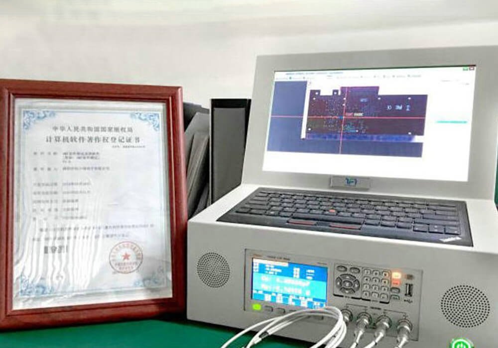
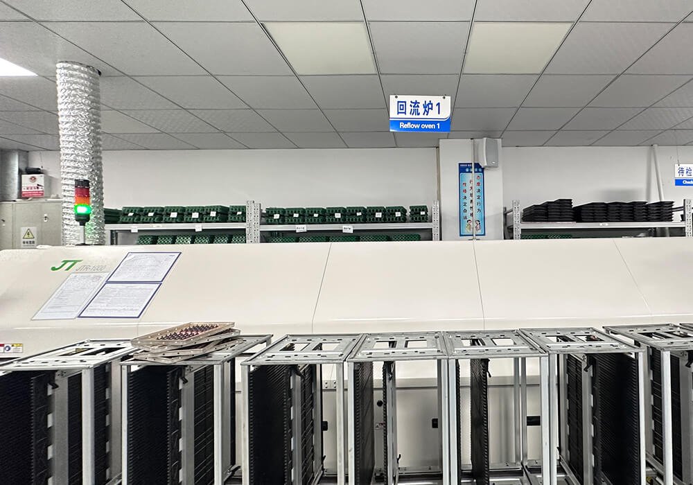
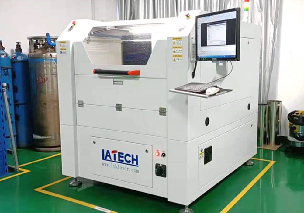
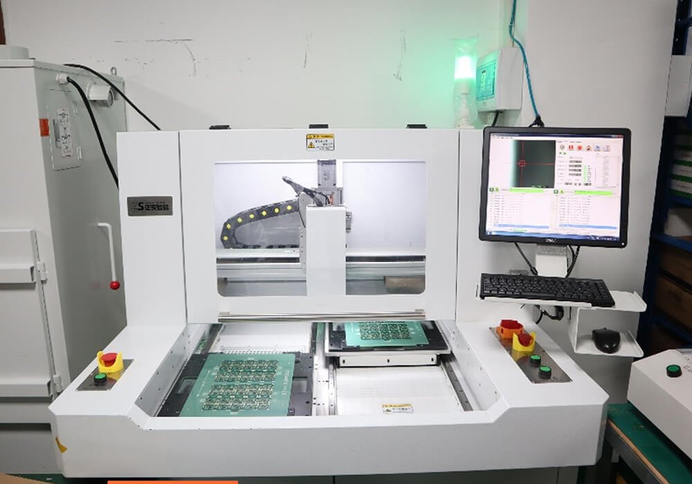
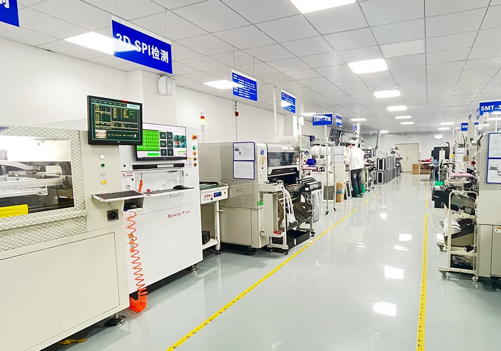
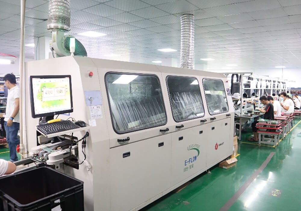
Our factory was equipped with automated SMT lines, intelligent process control systems, and advanced inspection equipment to support reliable PCB assembly from prototypes to high-volume production.

Wave Soldering Machine
Universal SMT Machine
SPI
Speed SMT Machine
Sample Tester
Reflow Oven
Laser Stencil Mach
KIC Oven Profiling System
Fully Automated PCB Depaneling Equipment
Automatic Printing Machine

Start Your Fine Pitch SMT Assembly Review

Send your current manufacturing package, target quantity, project stage, required date, and test expectations. We will review the available information, identify the questions needed for quotation, and define an appropriate manufacturing scope.

FAQ About Fine Pitch SMT Assembly

1. How do you reduce solder bridging?

Bridge control begins with pad and solder mask review. The assembly process then uses a suitable stencil aperture, stable paste printing, SPI, accurate placement and a qualified reflow profile. AOI detects visible bridges, while X-ray can reveal bridges beneath area-array packages.

No. Fine-pitch perimeter packages may route on conventional multilayer boards when pad spacing and breakout allow it. Dense BGA and CSP ball fields may require laser microvias or filled via-in-pad. The need for HDI depends on pitch, ball map, layer count, trace rules, stack-up and reliability requirements, not on the “fine pitch” label alone.

No. IPC class and X-ray coverage are separate requirements that must be defined for the product and contract. IPC-A-610 addresses post-assembly acceptance, while J-STD-001 covers soldering process and material requirements.