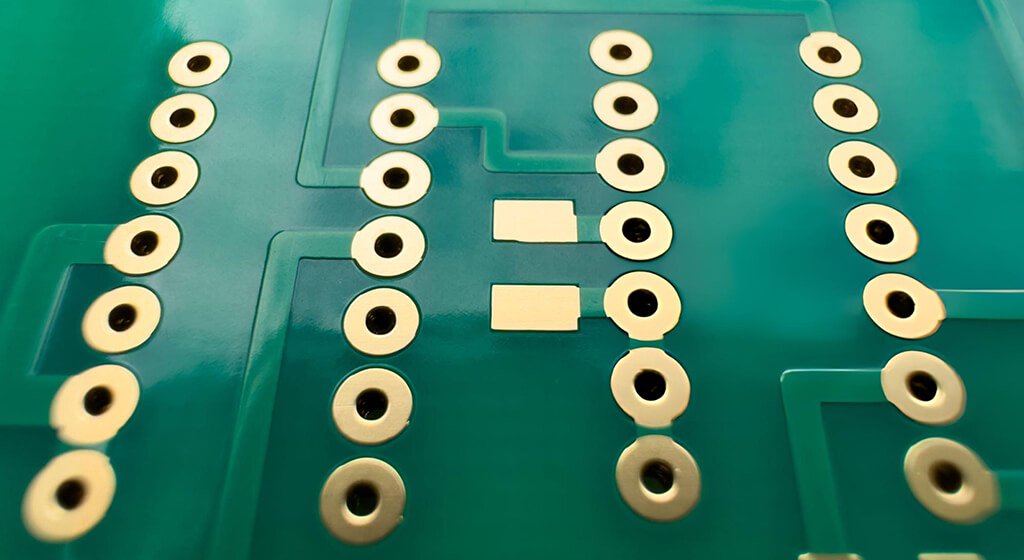
A PCB pad is an exposed conductive area used to solder, connect, test, or thermally couple a component to a printed circuit board.
Its final geometry should reflect the component terminal, manufacturer-recommended land pattern, solder mask, paste stencil, fabrication tolerances, assembly process, and reliability target.
No single PCB pad size formula works for every package or production line.
That boundary matters. A footprint can look correct in CAD yet remain difficult to etch, print, assemble, inspect, or repair. A reliable design treats the copper land, solder mask opening, and paste aperture as related but separate features.
Table of Contents
1. What Is a PCB Pad?
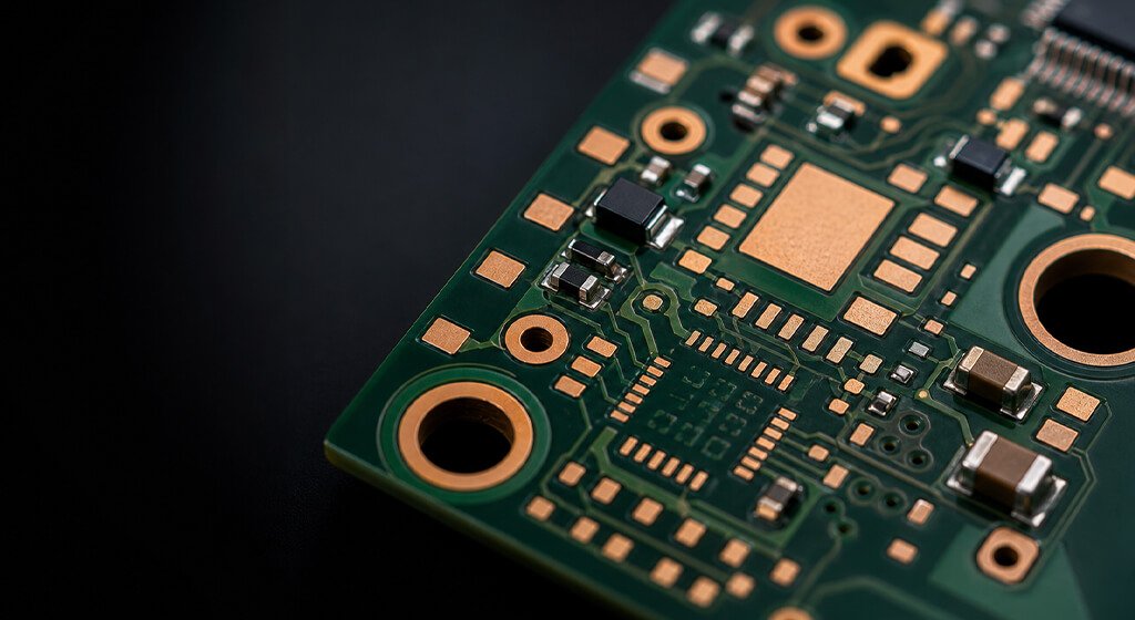
A PCB pad is a conductive feature that creates an electrical, mechanical, thermal, or test connection on a printed circuit board. Surface-mount pads receive component terminations directly. Through-hole lands surround drilled holes, while test pads provide probe access.
In standards work, land is often the more precise term, while pad remains common in ECAD tools and manufacturing discussions.
1.1. Pad, Land, Land Pattern, and Footprint
These terms overlap in everyday engineering conversations, but they do not describe the same thing:
- A land is a conductive surface feature intended for attachment or connection.
- A pad is the common ECAD and manufacturing term for that conductive feature.
- A land pattern is the complete board-side feature set needed to place and attach one component.
- A footprint is the ECAD library object. It can include lands, mask and paste definitions, courtyard data, assembly outlines, polarity marks, and reference text.
IPC-7352, Generic Guideline for Land Pattern Design defines a land pattern as the board area and features needed to place and attach a component.
It also states that generic guidance may require adjustment for company technology, board technology, and end-product requirements.
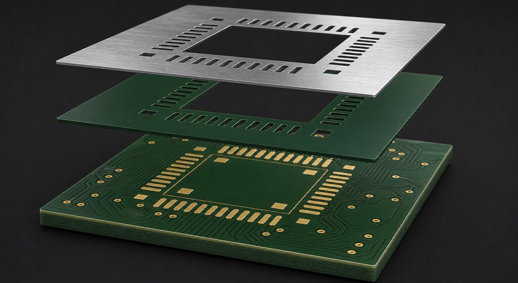
1.2. A PCB Pad Is a Three-Layer Geometry
For most surface-mount components, PCB pad design involves three independent geometries:
- Copper land: the conductive feature manufactured on the PCB.
- Solder mask opening: the exposed area around or inside the copper boundary.
- Paste aperture: the stencil opening that controls deposited solder paste.
Copying one shape to all three layers is not always correct. A chip resistor may use a paste aperture close to the copper geometry.
A large QFN exposed pad usually needs several smaller paste windows. A ball grid array may need a carefully controlled mask opening around each copper land.
2. Why Does PCB Pad Design Matter?
PCB pad design can influence:
- toe, heel, and side solder fillets;
- solder volume and component standoff;
- tombstoning and component rotation;
- pad cratering or lifting during mechanical stress;
- heat flow from an exposed package paddle;
- escape routing beneath BGA and wafer-level packages;
- automated optical inspection and X-ray coverage;
- probe access, rework access, and field reliability.
A pad that is too small may limit wetting or joint area. A pad that is too large may draw solder away from the terminal or increase bridging risk. The correct result depends on the package, process, tolerances, and service environment.
The pad also connects design decisions made by different teams. The component engineer controls the selected package. The layout engineer creates the footprint. The PCB fabricator controls etching and solder mask registration. The assembler controls paste printing, placement, and reflow.
Problems often appear at the boundary between those responsibilities. For example, a mathematically adequate mask web may be below the fabricator’s stable production capability.
An open via in a thermal pad may be easy to fabricate but may drain solder during reflow.
3. What Are the Main Types of PCB Pads?
PCB pads are best classified by connection method and function, not only by shape.
The main groups are surface-mount lands, through-hole lands, area-array lands, thermal pads, via-in-pad structures, and test contacts.
Each group creates a different manufacturing constraint. The following table helps identify the controlling design question before dimensions are selected.
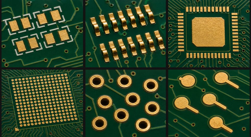
Pad Or Land Type | Primary Function | Main Design Control | Common Manufacturing Risk |
Chip-Component SMT Pad | Attach resistors, capacitors, and inductors | Terminal dimensions, fillet goals, paste balance | Tombstoning, solder beads, insufficient wetting |
Gull-Wing Or Leaded SMT Pad | Attach SOIC, QFP, and similar leads | Toe, heel, side allowance, lead tolerance | Bridging, lead misalignment, poor heel fillet |
QFN/DFN Perimeter Pad | Attach bottom terminations | Package drawing, mask strategy, stencil design | Opens, shorts under the body, weak side wetting |
Exposed Thermal Pad | Transfer heat and often current | Datasheet net, paste coverage, thermal vias | Voiding, floating, solder loss into vias |
BGA/WLCSP Land | Attach solder balls or bumps | Ball diameter, pitch, SMD/NSMD choice, escape routing | Opens, bridging, pad cratering, mask encroachment |
Through-Hole Land | Support a plated hole and solder joint | Finished hole, annular ring, lead fit, plating | Breakout, poor barrel fill, lifted land |
Via-In-Pad | Connect a pad directly to other layers | Via type, fill, cap, planarity, plating | Solder wicking, voids, uneven component seating |
Test Pad | Provide electrical probe access | Probe type, spacing, finish, keepout | Poor contact, probe damage, inadequate access |
Pad names do not set dimensions. A “BGA pad” could serve a 1.27 mm pitch package, a 0.4 mm pitch device, or a wafer-level component. Those cases have different routing, mask, and reliability limits.
4. What Is the Difference Between SMD and NSMD Pads?
Solder-mask-defined (SMD) pads use a mask opening smaller than the copper land, so the mask defines the solderable area.
Non-solder-mask-defined (NSMD) pads use a mask opening larger than the copper land, so etched copper defines the solderable area.
NSMD is common for many BGA and WLP packages, but neither construction is universally superior.
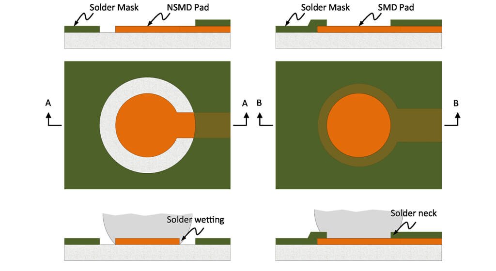
Decision Factor | SMD Pad | NSMD Pad |
Solderable Boundary | Defined by the solder mask opening | Defined by the copper land |
Copper Relationship | Mask overlaps the copper edge | Mask clears the copper edge |
Typical Advantage | Larger anchored copper feature; useful for selected packages or underfill strategies | Copper geometry often has tighter dimensional control; solder can wet the pad sidewall |
Main Constraint | Mask registration can change the exposed geometry | Requires enough mask clearance and web between neighboring lands |
Mechanical Consideration | Mask overlap may help retain the copper feature in some designs | Joint geometry can reduce some board-side stress concentrations |
Typical Use | Selected BGA, WLP, high-current, or application-specific footprints | Many BGA, WLP, QFN, and fine-pitch footprints |
Universal Default | No | No |
Several component manufacturers recommend NSMD for specific package families.
For example, TI’s AN-1112 DSBGA guide favors NSMD in its stated package context. Analog Devices’ WLP guidance also recommends NSMD for the WLP designs it covers.
Those recommendations should not become a universal rule. TI report SLVA430 documents a 0.4 mm DSBGA evaluation in which an SMD configuration produced the best assembly success rate among the tested boards.
Infineon also presents SMD and NSMD as a package-level tradeoff involving underfill and mechanical performance in its BGA pad comparison.
Use the exact component drawing first. Then verify that the proposed mask web and registration are realistic for the chosen PCB process.
5. Which Parameters Control PCB Pad Design?
The correct PCB pad depends on component geometry, fabrication variation, assembly variation, and product loads.
Copper dimensions alone are not enough. Engineers must also define the mask opening, paste deposit, trace entry, via structure, surface finish, and inspection method.
Every numerical starting point should retain its package and process context.
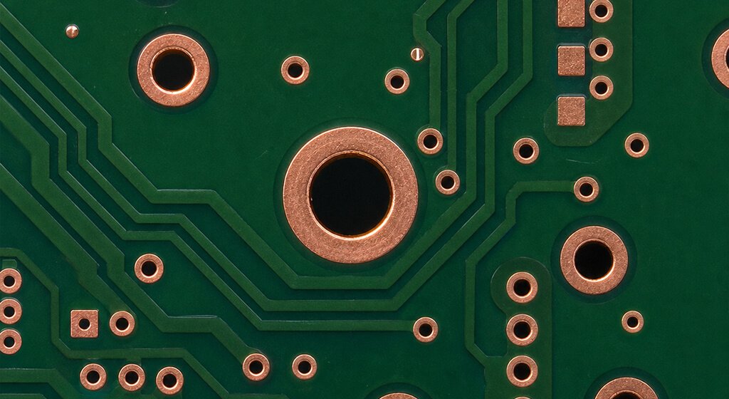
5.1. Component Termination and Tolerance
Start with the manufacturer part number, not a generic package name. Two components sold as QFN-32 may use different body sizes, terminal lengths, exposed pads, or tolerances.
Check the current datasheet for:
- terminal width, length, pitch, and tolerance;
- ball or bump diameter;
- exposed-pad dimensions and electrical connection;
- package coplanarity;
- the recommended land pattern and stencil notes;
- package drawing revision and manufacturing notices.
The recommended land pattern is normally the best starting point because the PCB package supplier knows the termination construction.
IPC guidance remains valuable when the datasheet is incomplete or when the design needs a documented tolerance analysis.
5.2. Copper, Mask, and Paste Relationship
Create and review the copper, mask, and paste layers separately. Confirm whether the ECAD library applies automatic mask expansion, because library defaults can silently overwrite a package-specific requirement.
The solder mask opening must accommodate registration variation without exposing unwanted copper. It must also leave a manufacturable mask web between adjacent pads. A fine-pitch footprint may require a different mask strategy if the remaining web cannot be produced consistently.
Paste volume depends on aperture area and stencil thickness. Area ratio compares the aperture opening area with its wall area.
For a rectangular aperture:
- Area ratio = (L × W) / [2t(L + W)]
Here,
- L and W are aperture dimensions,
- and t is stencil thickness.
An area ratio of at least 0.66 is a widely used printing rule of thumb, not a universal contractual limit.
Indium explains both the formula and this boundary in its stencil printing guidance. Paste formulation, powder size, aperture finish, nanocoating, printer setup, and cleaning frequency can change actual transfer efficiency.
5.3. Trace Entry and Solder Thieving
A trace entering an NSMD land creates extra wettable copper.
If the trace is too wide or asymmetrical, solder may wick away from the intended joint. This can alter ball shape, component rotation, and joint standoff.
Follow the component manufacturer’s trace-entry guidance when it is available. Teardrops may reduce local stress in some WLP designs, but they must not remove the clearance needed for routing or solder mask.
5.4. Vias, Thermal Paths, and Planarity
Do not place an open via inside a solderable pad without evaluating solder flow. During reflow, molten solder can move into the via barrel and leave an insufficient deposit under the component.
Possible treatments include:
- moving the via outside the solderable area;
- tenting the via where the process permits;
- plugging or filling the via;
- plating over and planarizing the filled via;
- using small encroached thermal vias with a tailored stencil pattern.
Via-in-pad plated over (VIPPO) is useful for dense area arrays, but it adds process steps and cost. Planarity, fill material, plating integrity, via depth, and acceptance criteria should be agreed with the fabricator.
5.5. Surface Finish and Copper Thickness
Surface finish influences solderability, planarity, storage life, wire bonding, contact wear, and cost.
ENIG, ENEPIG, OSP, immersion silver, immersion tin, and HASL do not provide identical pad surfaces.
Fine-pitch and area-array applications often value a flat finish, but the device supplier may impose additional restrictions.
Copper thickness also changes etching capability, finished pad geometry, thermal spreading, and solder-joint standoff.
Do not copy a pad from a thin-copper prototype into a heavy-copper design without review.
6. How Do You Determine the Correct PCB Pad Size?
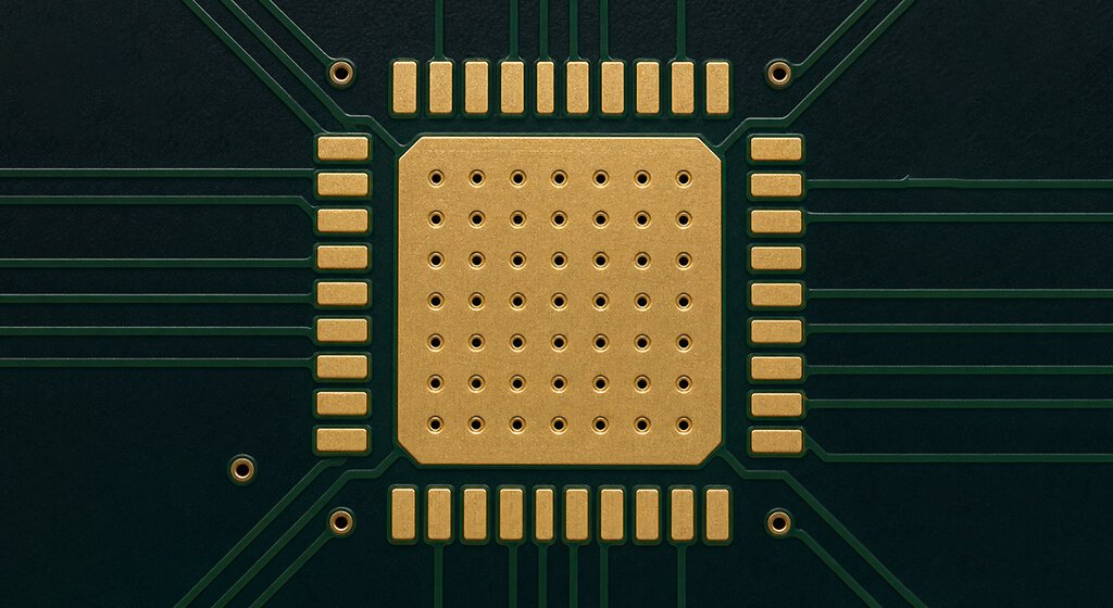
There is no reliable one-line calculation for every PCB pad.
A defensible method begins with the exact component drawing, adds fabrication and placement tolerances, defines the intended solder joint, and checks mask and stencil capability.
It ends with fabricator and assembler DFM, followed by first-build inspection. The workflow below is more reliable than copying a generic footprint.
- Confirm the manufacturer part number. Include package suffixes because they can identify different terminal constructions.
- Download the current datasheet and package drawing. Record the revision used to build the library.
- Import or calculate the recommended land pattern. Do not assume a distributor symbol or community library is correct.
- Check component and board tolerances. Include terminal variation, copper etch variation, mask registration, placement accuracy, and board scaling where relevant.
- Design copper, mask, and paste independently. Document the SMD/NSMD decision and any package-specific exceptions.
- Review routing and vias. Check trace entry, escape routing, thermal vias, via fill, and copper balance.
- Run fabrication and assembly DFM. The board shop and assembler must evaluate the same footprint against their real processes.
- Validate the first build. Use solder paste inspection (SPI), automated optical inspection (AOI), X-ray, electrical testing, cross-sections, or reliability testing according to risk.
A useful pre-release process also checks pin mapping, polarity, courtyard spacing, test access, and assembly drawings.
7. How Do Pad Decisions Change by Package and Application?
Package construction changes the controlling pad risk. Chip components need balanced solder forces.
Gull-wing leads need suitable toe and heel geometry.
QFN and DFN packages require coordinated perimeter pads, exposed-pad paste, and thermal vias.
BGA and WLCSP designs depend on ball geometry, mask strategy, escape routing, and hidden-joint inspection. Through-hole lands depend on finished-hole and annular-ring requirements.

7.1. Chip Components and Gull-Wing Leads
For chip resistors and capacitors, unequal pad geometry or unequal thermal connection can promote tombstoning. Paste deposits and copper connections should be balanced where the electrical design allows.
For SOIC, QFP, and other gull-wing packages, the land must support the required toe, heel, and side joint geometry. Excessive toe length consumes space and can encourage solder movement without improving every reliability condition.
7.2. QFN, DFN, LGA, and Exposed Pads
The exposed pad may serve a thermal, electrical, mechanical, or combined function. Do not automatically connect it to ground.
Analog Devices’ exposed-pad guidance directs designers to the device datasheet for the required electrical connection.
Large exposed pads usually use multiple paste apertures. However, recommended coverage varies by package and process.
Microchip AN18.15 gives a 65% to 90% exposed-pad range and a narrower 70% to 75% target for its encroached-via example. Analog Devices gives a 50% to 80% range in its standard QFN assembly guide.
These ranges are manufacturer guidance, not universal acceptance limits.
The stencil pattern should reflect via placement, paste behavior, reflow profile, void target, package standoff, and thermal requirement. IPC-7093A provides the broader bottom-termination component implementation framework.
7.3. BGA and WLCSP
BGA pad size should be derived from the package supplier’s ball data and land recommendation. The pad also affects how many traces can escape between neighboring balls. Reducing a pad only to gain routing space may weaken assembly margin.
Hidden joints require an inspection plan. AOI can inspect placement and visible features, but it cannot directly see the solder connection under a BGA body. X-ray can reveal many bridging, voiding, and alignment conditions, although it cannot prove every joint is reliable. IPC-7095E covers BGA design, assembly, inspection, rework, and troubleshooting at the process level.
Fine-pitch packages may require microvias or filled via-in-pad structures.
The feasibility of those structures should be reviewed as part of HDI PCB manufacturing, not after routing is complete.
7.4. Through-Hole and Test Lands
A through-hole land must provide a finished hole that accepts the lead while preserving the required annular ring after drilling and plating variation.
Lead fit, hole tolerance, copper plating, solder access, and assembly method all affect the result.
IPC-2221C supplies generic design requirements, while IPC-6012F and IPC-A-600M address rigid-board performance and bare-board acceptability. Assembly requirements then come from IPC J-STD-001 and IPC-A-610.
Projects that use connectors, transformers, or mechanically loaded parts should also review the planned through-hole PCB assembly process.
Test pads require a different analysis. Their diameter, pitch, finish, keepout, and access angle should match the selected probe technology. A pad that is accessible to a handheld probe may still be unsuitable for a production fixture.
7.5. Power, RF, and Flex Applications
High-current pads may need wide copper entry or multiple connections that conflict with generic solder-thieving advice.
Thermal pads may need extensive copper and via arrays.
RF pads can be part of an impedance transition, so pad capacitance, mask coverage, and launch geometry require electromagnetic analysis.
Flex circuits add bend location, coverlay registration, adhesive squeeze-out, and pad anchoring concerns. Keep component pads away from dynamic bend zones unless the construction is specifically qualified for that use.
8. How Does a CAD Pad Become a Manufactured Solder Joint?
A PCB pad passes through several processes before it becomes a solder joint.
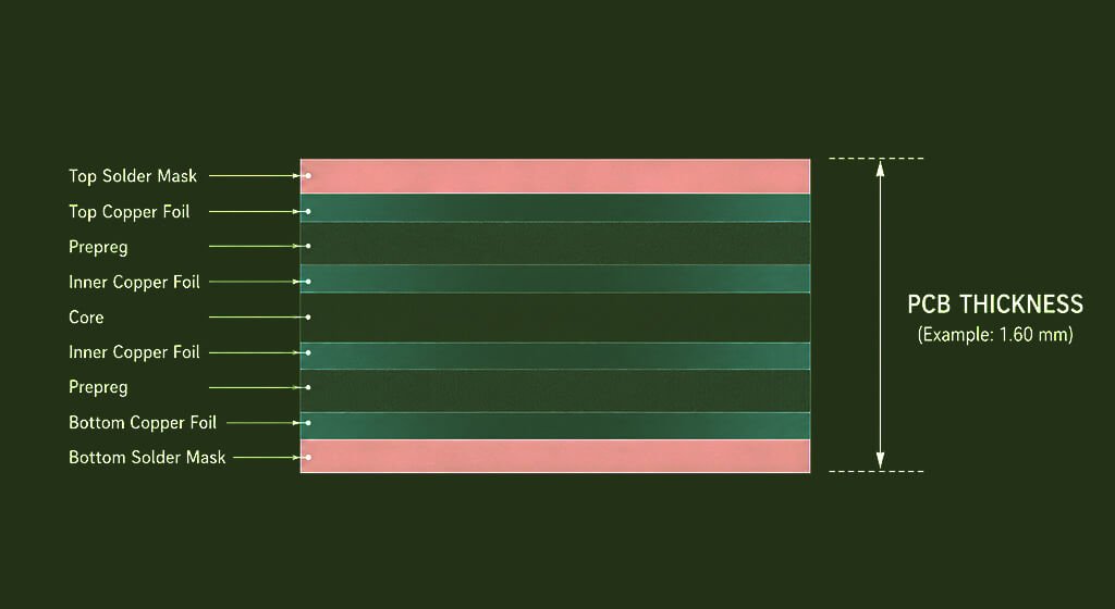
Copper is imaged and etched, solder mask is registered and developed, and the selected finish is applied.
The assembler then prints paste, places the component, and runs reflow.
Each stage adds variation, so the final solderable geometry will not be a perfect copy of the nominal CAD shape.
A typical sequence is:
- ECAD footprint release and CAM data preparation.
- Copper imaging, etching, plating, and feature inspection.
- Solder mask coating, imaging, development, and cure.
- Surface-finish processing and bare-board inspection.
- Stencil fabrication from the approved paste layer.
- Paste printing and SPI where specified.
- Component placement and reflow soldering.
- AOI, X-ray, electrical test, and functional test as required.
IPC-7525C provides stencil design guidance, but its public scope notes that printing depends on many variables. It does not establish one rule set for every product.
For surface-mount projects, review pad and paste decisions with the intended SMT assembly process before releasing the stencil.
Changing a stencil is cheaper than rebuilding an assembled batch, but a stencil change cannot correct a fundamentally wrong copper footprint.
9. What PCB Pad Defects Occur, and How Are They Prevented?
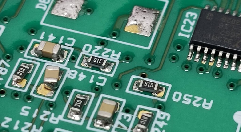
PCB pad defects often result from interactions rather than a single bad dimension.
Copper geometry, mask registration, paste transfer, component tolerance, reflow, via design, and handling can combine to create the failure.
Effective troubleshooting identifies the defect mechanism, confirms it with suitable inspection, and corrects the responsible design or process variable instead of enlarging every pad.
Defect | Likely Causes | Useful Detection Method | Design Or Process Response |
Solder Bridging | Excess paste, tight spacing, mask loss, placement error | SPI, AOI, X-ray for hidden joints | Reduce or reshape aperture; review spacing, mask, placement, and reflow |
Insufficient Solder Or Open Joint | Poor paste release, small aperture, contamination, solder wicking | SPI, AOI, X-ray, electrical test | Check area ratio, paste, finish, via treatment, and profile |
Tombstoning | Unequal paste, pad geometry, copper connection, or heating | AOI and visual inspection | Balance pad geometry, paste deposits, copper entry, and thermal mass |
QFN Exposed-Pad Voiding | Large paste opening, trapped volatiles, via layout, reflow profile | X-ray; cross-section when needed | Use window apertures; adjust via pattern, paste, and reflow |
Solder Loss Into Via | Open or poorly treated via-in-pad | X-ray, cross-section, electrical or thermal test | Move, tent, plug, fill, cap, or redesign the via |
Solder Mask Encroachment | Inadequate expansion or registration margin | Bare-board AOI and microscopy | Increase clearance or change SMD/NSMD strategy |
Lifted Or Damaged Pad | Excess rework heat, force, weak anchoring, laminate damage | Visual inspection, microscopy, continuity test | Control rework; repair under an approved procedure; reassess mechanical load |
BGA Open Or Head-In-Pillow | Warpage, oxidation, paste condition, placement, reflow | X-ray, electrical test, dye-and-pry or cross-section for investigation | Correct storage, paste, profile, board support, and package process |
Do not treat AOI as proof of hidden-joint quality. Our guide to AOI limits and complementary inspection methods explains how SPI, AOI, X-ray, in-circuit test, and functional test address different risks.
If a pad has already lifted, the correct action depends on damage depth, electrical function, product class, and customer authorization.
IPC-7711/21D provides controlled rework and repair procedures. A repair should not be improvised from a generic online illustration for a high-reliability product.
10. Why Are Generic PCB Pad Rules Not Enough?
Generic rules are useful starting points, but they cannot capture every package, board construction, assembly line, or service condition.
The same nominal pitch can use different ball sizes and tolerances. A mask web that works on one process may fail on another.
Prototype capability may also differ from a stable, documented production window.
IPC-7352 explicitly allows adjustments for company and board technology.
It also notes that shock and vibration effects are outside its generic treatment.
A land pattern suitable for a benign consumer device may therefore need additional qualification for automotive, aerospace, industrial, or portable equipment.
The manufacturing supplier should review:
- copper feature size after the selected copper weight and finish;
- solder mask opening, web, registration, and ink process;
- drilling, microvia, fill, cap, and planarity capability;
- stencil thickness, aperture release, and paste selection;
- placement accuracy, board support, and reflow profile;
- inspection coverage and product acceptance criteria;
- expected volume, because an engineering limit is not always a production limit.
11. What Should Engineers Check Before Releasing PCB Pads?

A release checklist should confirm source data, geometry, manufacturability, assembly, and verification. It should also document exceptions.
The goal is not to prove that a CAD library follows one generic formula. The goal is to show that the selected footprint can produce the intended solder joint within the actual fabrication and assembly process.
- The exact manufacturer part number and package suffix are confirmed.
- The current datasheet, package drawing, and land recommendation are archived.
- Symbol pins, footprint pads, and package terminals have been cross-checked.
- Copper, solder mask, and paste layers were reviewed separately.
- The SMD or NSMD choice is documented for area-array packages.
- Pad dimensions include the intended component and manufacturing tolerances.
- Trace entry does not create unwanted solder thieving or asymmetry.
- The exposed pad’s electrical net is confirmed from the device datasheet.
- Thermal vias and via-in-pad structures have an approved fill or tent strategy.
- The remaining solder mask web is within the fabricator’s production capability.
- Surface finish matches soldering, storage, contact, and reliability needs.
- IPC class and customer acceptance criteria are stated on the documentation.
- SPI, AOI, X-ray, electrical test, and functional test coverage are risk-based.
- Rework access, probe access, polarity marks, and component courtyard are adequate.
- Both the PCB fabricator and PCBA assembler completed DFM review.
12. How Can PCBSAIL Help With PCB Pad and Land-Pattern DFM?
We can review PCB pad data across fabrication and assembly, where many land-pattern failures originate.
The review can identify mismatches among copper, solder mask, paste apertures, vias, routing, and inspection access.
It should use the actual stackup, copper weight, component data, production volume, and acceptance requirements. Final process limits and inspection coverage remain project-specific.
12.1. Manufacturing Risks PCBSAIL Can Review
A PCB pad review should target a defined failure mechanism rather than apply a generic footprint rule.
We can review the supplied manufacturing package for risks such as:
- a footprint that does not match the selected manufacturer part number or package revision;
- solder mask openings that leave an unstable web or insufficient registration margin;
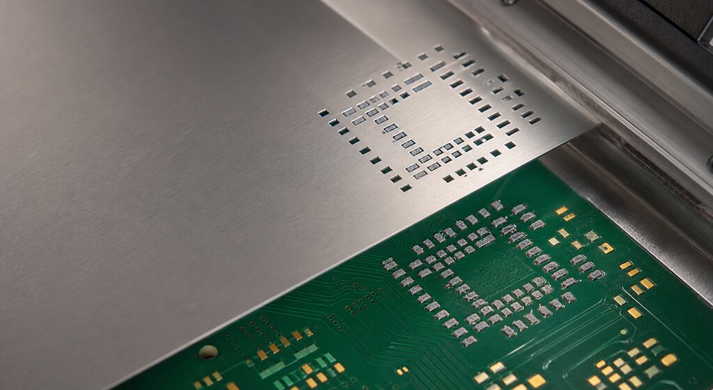
- paste apertures that create poor transfer, excessive solder, tombstoning, or bridging risk;
- open or unsuitable via-in-pad structures that can drain solder during reflow;
- QFN or DFN exposed-pad designs with uncontrolled paste coverage or thermal-via interaction;
- BGA and WLCSP escape routing that conflicts with pad, mask, or microvia geometry;
- through-hole finished-hole and annular-ring relationships that do not suit the component lead;
- pad and test-point layouts that cannot be inspected, probed, or reworked as intended.
13. FAQ About PCB Pads
How do you calculate PCB pad size?
Start with the exact component manufacturer’s land recommendation. Then account for terminal tolerance, intended solder fillets, copper fabrication tolerance, solder mask registration, paste printing, and placement variation. IPC-7352 provides a generic framework, but no single equation covers every surface-mount, through-hole, thermal, or area-array pad.
Should a PCB pad be larger than the component terminal?
Sometimes, but not always. Gull-wing and chip-component lands often include allowances that support visible solder fillets. BGA and WLP lands may be similar to or smaller than the ball diameter. The correct relationship depends on termination style, solder volume, joint shape, pitch, and reliability objective.
How large should the solder mask opening be?
The opening must expose the intended solderable area while accommodating mask registration and preserving a manufacturable web. The required expansion depends on whether the pad is SMD or NSMD, the pitch, mask process, board supplier, and product requirements. A generic expansion should not override the package drawing or approved DFM rules.
Can a via be placed inside a PCB pad?
Yes, but the via structure must suit assembly. An open via can draw solder away from the joint. Dense BGA designs often use filled, capped, and plated-over vias, while some exposed thermal pads use small open or encroached vias with a tailored paste pattern. Confirm fill, cap, planarity, void, and inspection requirements.
References
– [IPC-7352: Generic Guideline for Land Pattern Design]
– [IPC official document revision table]
– [IPC-2221C: Generic Standard on Printed Board Design]
– [IPC-6012F: Qualification and Performance Specification for Rigid Printed Boards]
– [IPC-A-600M: Acceptability of Printed Boards]
– [IPC-7525C: Stencil Design Guidelines]
– [IPC-7093A: Bottom Termination Components]
– [IPC-7095E: Ball Grid Arrays]
– [IPC J-STD-001J: Requirements for Soldered Assemblies]
– [IPC-A-610J: Acceptability for Electronic Assemblies]
– [TI AN-1112: DSBGA Wafer-Level Chip-Scale Package]
– [TI SLVA430: 0.4 mm DSBGA Board Design Evaluation]
– [Microchip AN18.15: PCB Design Guidelines for QFN and DQFN Packages]
– [Analog Devices: Wafer-Level Packaging and Its Applications]
– [Analog Devices: Exposed Pads—A Brief Introduction]
– [Analog Devices: SMT Assembly and PCB Design Guidelines for Standard QFN Packages]
– [Infineon: SMD and NSMD Pad Types for BGA Packages]
– [Indium: Stencil Printing Metrics and Area Ratio]