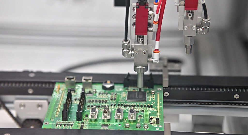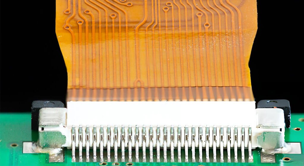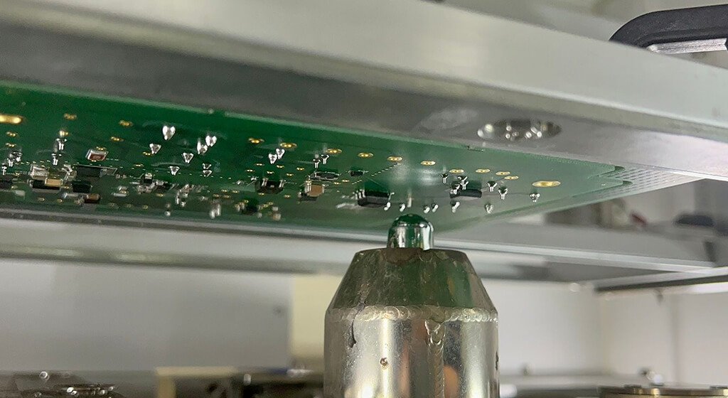
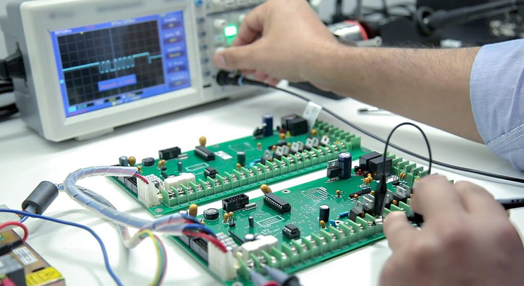
SMT testing is used in inspection with electrical verification during the PCB assembly.
It takes a close look at printed solder paste, component placement, solder joints, electrical connections, and how the board behaves when powered up. Each testing method addresses a unique aspect of your assembled board.
Sometimes, a board might appear to be in perfect shape but could still have an incorrect resistor value lurking beneath the surface. Hidden solder bridges can easily slip past optical inspections, and a quick startup check might overlook interface failures. That’s why your SMT testing should incorporate various types to specific risks.
This guide dives into the different testing and inspection methods. You’ll discover how to compare these methods, set acceptance criteria, and create a practical test plan. Plus, it also explains what passing results prove and how to handle failures.
Key Takeaways:
- Process inspection evaluates physical manufacturing conditions; electrical tests measure circuit characteristics.
- Hidden solder joints require inspection methods suited to their geometry.
- Test access and program design determine useful electrical coverage.
- A passing functional test covers only the specified behaviors and conditions.
Table of Contents
1. What Does SMT Testing Include?
SMT testing includes physical inspections, electrical measurements, and assessments of powered operation. Your test plan combines these methods according to the board’s risks and acceptance requirements.
Solder paste inspection (SPI), automated optical inspection (AOI), and X-ray examine manufacturing conditions.
In-circuit testing (ICT) and flying probe tests focus on measuring specific electrical characteristics, while functional testing checks specified operating behavior.
1.1. Process Inspection
Process inspection focus on the physical state of materials, components, and solder joints while they’re being assembled.
Solder paste inspection (SPI) focuses on assessing the printed deposits before any components are put in place.
Automated optical inspection (AOI) checks visible placement and solder features. X-ray inspection examines joints hidden beneath component bodies.
Whenever an inspection flag pops up, it’s crucial to review it against the relevant acceptance criteria.
For instance, if there’s a visible solder issue, it might need fixing even if the circuit is still functioning properly.
1.2. Electrical Testing
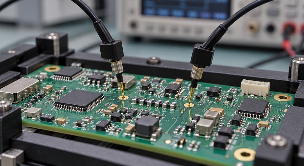
Electrical testing measures circuit connections and selected component characteristics on an assembled board.
In-circuit testing (ICT) and flying probe testing can detect opens, shorts, and some incorrect component values. The actual coverage depends on test access, circuit paths, and the programmed measurements.
What sets these methods apart is the way they interact with the board and carry out their measurements.
These methods differ in how they contact the board and perform measurements. Keysight’s test-options guide explains their capabilities and access constraints.
1.3. Functional Testing
Functional circuit testing (FCT) checks whether a powered assembly performs its specified functions under defined conditions..
Your testing process might involve checking things like startup, communication, sensor responses, or how the outputs behave when there’s a load. It’s important to clearly define the firmware, supply conditions, test inputs, and the criteria for passing or failing.
National Instruments (NI) offers guidance on production testing, which includes setting up functional test stations based on specific product requirements.
These tests are focused on the assembled board. Bare-board testing checks the fabricated PCB before components are fitted. Printed circuit board assembly (PCBA) testing also evaluates component installation, solder connections, and specified circuit behavior.
2. Where Does Each Test Fit in the SMT Assembly Process?
SMT inspection starts after solder paste printing and continues through placement and reflow. Once the assembly operations are complete, we move on to electrical and functional tests tailored for each specific test.
Your board’s package types, manufacturing risks, and acceptance requirements determine the checkpoints. Not every production line needs every inspection station, and some checks need to be done before shielding or coating, as those can limit access.

2.1. After Solder Paste Printing
Solder paste inspection (SPI) normally takes place after stencil printing and before component placement.
This step is crucial because it allows you to catch any issues with the paste deposits while there’s still time to fix them without without removing components.
If you notice problems like insufficient paste, too much volume, or misaligned deposits, it could indicate a printing issue. Based on what you find, your team might need to clean the stencil, correct alignment, or review paste handling.
Remember, any affected board needs an approved disposition before placement continues.
2.2. Before Reflow Soldering
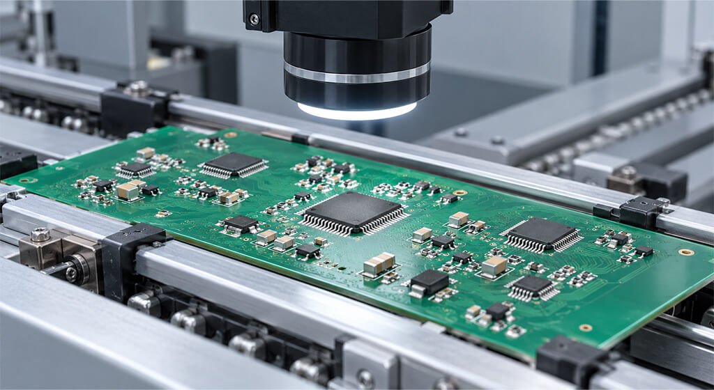
Before the solder joints are formed, pre-reflow automated optical inspection (AOI) checks component placement.
If there are clear visual features to work with, it can identify missing parts, misaligned placements, and incorrect orientations.
This step is crucial because it allows placement errors to be corrected before soldering.
However, it’s important to note that it can’t assess the final joints quality ince the solder hasn’t been reflowed yet.
2.3. After Reflow Soldering
Post-reflow AOI checks visible components and solder joints after the board has cooled sufficiently for inspection. If there are hidden joints that need a closer inspection, like those under a ball grid array (BGA) package, X-ray inspection can be added to the process.
Here’s a typical inspection sequence you might follow:
Printing → SPI → Placement → Pre-reflow AOI, if specified → Reflow → Post-reflow AOI → X-ray, if specified
According to OMRON’s SMT process, SPI, placement inspection, and post-reflow inspection are positioned at these specific stages. It’s important for your production plan to clearly outline which stations are used and what each station checks.
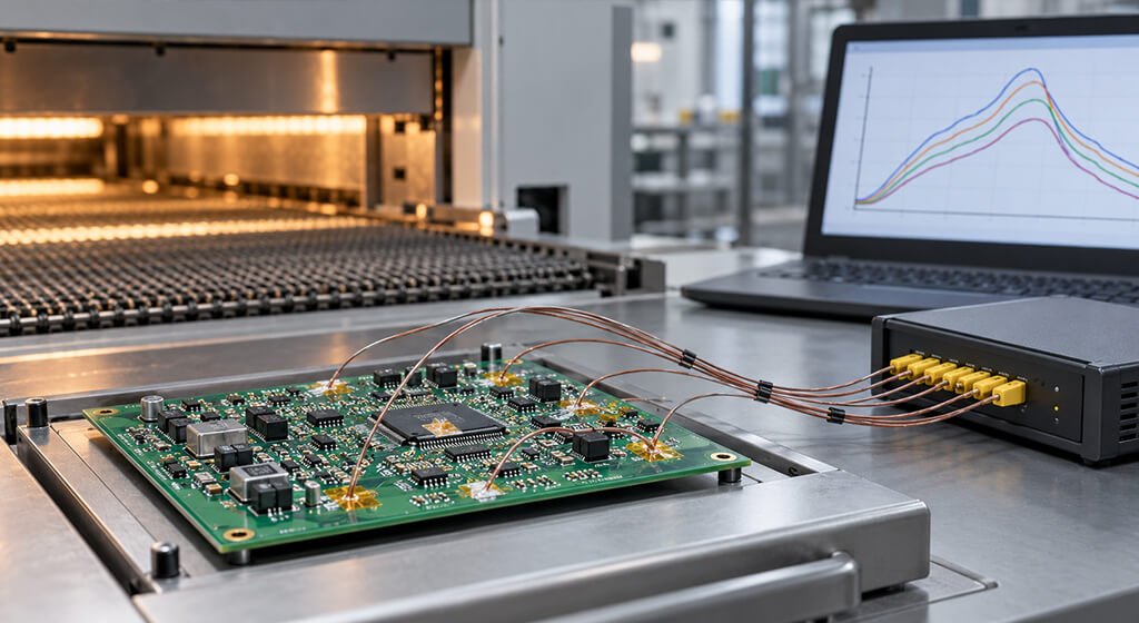
Thermocouples placed at chosen spots on the board track the temperature during both the heating and cooling phases. These readings are crucial for confirming the thermal profile, but they do not replace inspection of the finished joints. For more details, refer to the KIC profiling manual, “Attaching thermocouples.”
2.4. During Post-Assembly Electrical Verification
Electrical verification takes place once the connections needed for that test are assembled.
Your sequence may include in-circuit testing (ICT), flying probe testing, programming verification, and functional circuit testing (FCT). Their order depends on test access, programming needs, and the approved procedure.
If your board has through-hole components, you might need to conduct final electrical acceptance after those soldering tasks are completed.
While earlier checks offer valuable insights into the process, they won’t be able to confirm connections that were added later on.
3. Common SMT Inspection and Testing Methods
When it comes to SMT inspection and testing, there are several methods that focus on various aspects of assembly quality.
Visual inspection, SPI, AOI, and X-ray are great for assessing physical features. ICT and flying probe are used to measure specific electrical characteristics, while FCT focus on how the board behaves when powered.
For your board, the useful combination depends on joint visibility, electrical access, coverage, and production.
Method | Typical stage | Useful checks | Required preparation | What passing does not prove |
Visual inspection | First-article, manual-operation, or final review | Visible workmanship and mechanical assembly | Drawings, lighting, access, criteria | Hidden-joint integrity or circuit function |
SPI | After printing | Paste height, area, volume, and position, depending on system | Pad data and validated limits | Final solder-joint acceptance |
AOI | After placement or reflow | Visible placement and solder features | Program, libraries, review criteria | Electrical values or hidden connections |
X-ray | Usually after reflow | Hidden solder structure | Suitable imaging and package criteria | Complete electrical performance |
ICT | After required assembly | Accessible electrical faults and selected values | Test access, program, usually a fixture | Complete product operation |
Flying probe | After required assembly | Selected accessible nets and values | Contact targets and test program | Untested nodes or behaviors |
FCT | At a defined powered stage | Specified operating behavior | Firmware, loads, equipment, limits | Untested functions or lifetime reliability |
3.1. Visual Inspection
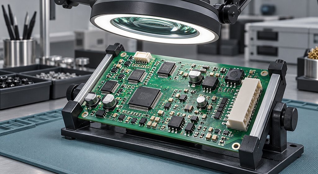
Visual inspection plays a important role when it comes to features that are difficult to assess automatically.
Your inspector can take a close look at things like connector seating, damaged packages, cable routing, and exposed solder joints.
While using magnification can be beneficial, it’s essential to ensure there’s a clear viewing angle for the feature being inspected.
To make consistent decisions, the right lighting and well-documented acceptance criteria is key. An approved reference board can help explain an acceptable condition. If it conflicts with the released drawing or specification, the discrepancy needs resolution.
3.2. Solder Paste Inspection (SPI)

Three-dimensional SPI systems are great for measuring deposit height, volume, area, and position. These measurements help identify printing variation before components cover the deposits.
Your limits should reflect pad geometry and the validated printing process. A small component pad and a large thermal pad may need different settings. pSemi recommends inspecting printed paste before placement.
3.3. Automated Optical Inspection (AOI)
AOI uses cameras, controlled lighting, and programmed criteria to assess visible assembly features. It can identify offset, polarity errors, and solder bridges. It can also detect tombstoning, where a chip component stands on one end.
When it comes to verifying component identity, AOI relies on readable markings or other unique features. Similar-looking unmarked parts may remain indistinguishable. AOI also cannot directly inspect solder balls hidden beneath a BGA package.
Whenever an AOI found an issue, it’s essential to document the findings against the acceptance criteria. If false calls happen repeatedly, it’s time to take a closer look at the imaging, libraries, and thresholds. Just it isn’t a good fix that broadening the limits, as it might let genuine defects slip through the cracks.
3.4. X-Ray Inspection and Automated X-Ray Inspection (AXI)
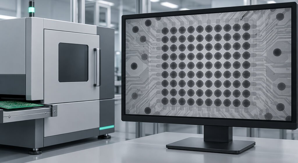
PCB assembly X-ray inspection produces images from differences in X-ray absorption through the assembly. It can reveal hidden solder distribution, bridges, and voids. Automated X-ray inspection (AXI) uses programmed image acquisition and evaluation for specified inspection tasks.
With two-dimensional projections, you can layer features from both sides of a board, while oblique views or computed tomography (CT) can clarify features that might otherwise be confusing. Nordson offer these image acquisition options in its inspection systems.
When selecting a technique, it’s crucial to ensure it has the right resolution and for the target defect. Keep in mind that even a clear image doesn’t guarantee complete electrical performance or metallurgical bond quality.
3.5. In-Circuit Testing (ICT)
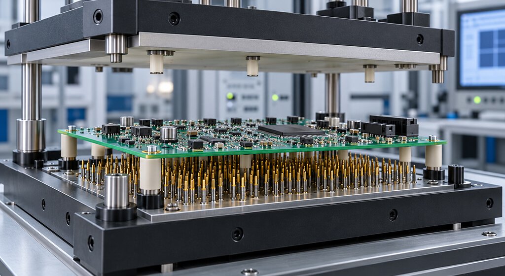
In-circuit testing (ICT) evaluates circuit nodes and component characteristics by planned electrical access. A traditional bed-of-nails fixture can connect with multiple targets all at once during a single fixture engagement. After that, the test program carries out the necessary measurements.
ICT encompasses both unpowered and powered test. “Unpowered” means the board lacks its normal operating supply; measurement stimuli still apply. Keysight distinguishes between shorts and analog in-circuit checks, separating them from powered digital and analog tests.
When setting your test limits, it’s essential to consider component tolerances and the surrounding circuit paths. Just the equipment measurement ranges alone do not define acceptable board behavior.
3.5. Flying Probe Testing
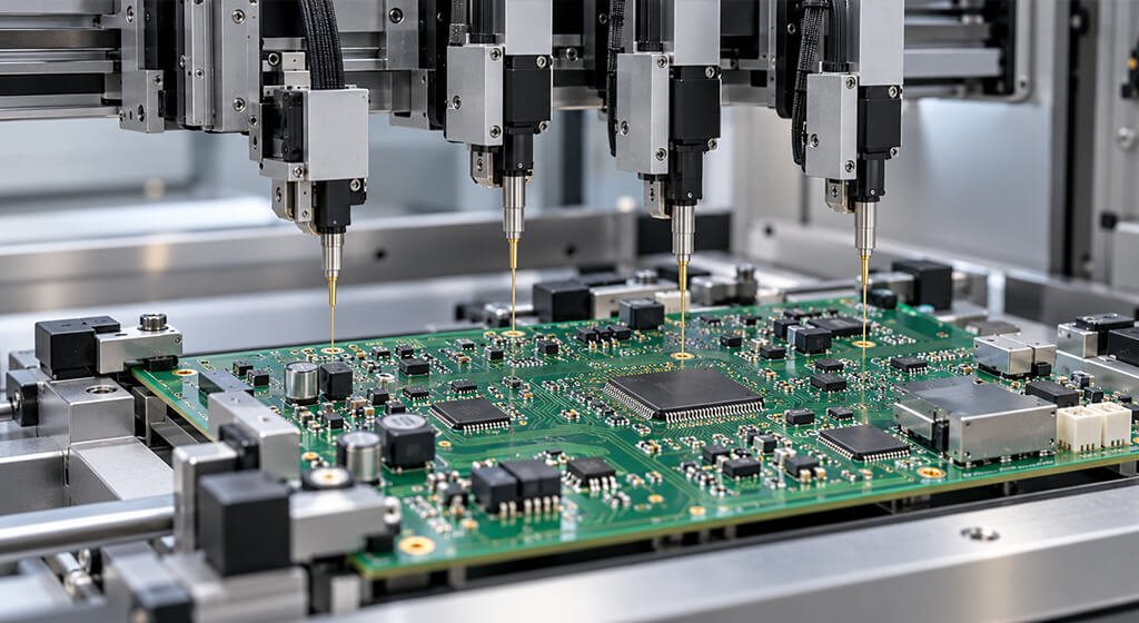
Flying probe are designed to navigate between accessible targets to carry out programmed electrical measurements. They avoid a dedicated bed-of-nails fixture, although board support and suitable contact locations remain necessary.
This adaptability makes them ideal for prototypes and designs that are still evolving. Actual test time depends on probe travel, measurements, settling time, and program structure. It’s essential for your PCBA supplier to verify that they can cover the populated board, as bare-board test capability doesn’t guarantee coverage for assembled boards.
3.6. Functional Testing (FCT)
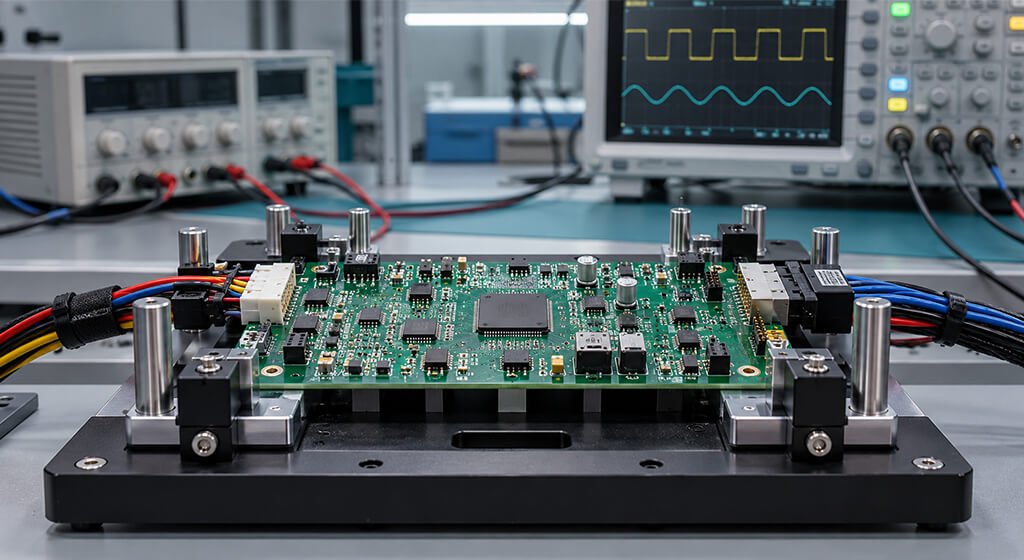
PCBA functional testing checks operating behavior against the product specification. Depending on your board, it may verify supply current, interface responses, sensor readings, or outputs under load.
A useful procedure specifies the firmware, stimulus, load, expected response, and pass/fail limits. A board that boots successfully may still fail a communication or load test. You need to check those behaviors when required for acceptance.
NI offers functional test stations that are designed around set product specifications. Their hardware and software are tailored to handle the necessary measurements and production conditions.
4. Which SMT Defects Can Each Method Detect?
The SMT Testing method depends on the defect and the available access.
AOI can reveal visible placement errors, while X-ray can expose hidden solder abnormalities. Electrical measurements help identify opens, shorts, and incorrect values; functional tests reveal failures during operation.
Often, you need to use a combination of these methods to pinpoint the problem and figure out the best fix.
Issue | Useful initial method | Condition affecting detection | Follow-up decision |
Missing visible component | AOI or visual review | Visibility and correct population data | Confirm whether the location should be populated |
Suspected bridge beneath a package | X-ray | Image resolution, viewing angle, and overlapping structures | Check electrical evidence where accessible; apply joint acceptance criteria |
Open connection | ICT or flying probe | Node access, parallel paths, and test-program coverage | Isolate the affected connection before rework |
Incorrect resistor value | Electrical measurement | Neighboring components and measurement isolation | Confirm the reading before replacing the component |
Abnormal hidden-joint shape | Suitable X-ray imaging | Package geometry and inspection criteria | Request additional views or engineering review if uncertain |
Communication failure | FCT | Firmware, power, timing, cables, and interface setup | Verify the test setup before tracing the board-level fault |
4.1. Missing or Misplaced Components
AOI or visual inspection can identify missing and misplaced parts when the relevant features are visible. Your inspection data must distinguish missing components from locations intentionally left unpopulated.
A shifted component does not always cause an immediate electrical failure. Its position still needs to meet the applicable assembly criteria. Conversely, correct placement does not confirm the component’s value or internal condition.
4.2. Solder Bridges and Open Connections
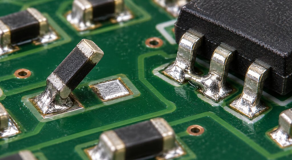
Visible solder bridges may be detected optically, while bridges beneath packages may require X-ray imaging. ICT or flying probe can detect a short when the relevant nodes are accessible and included in the program.
An open-circuit indication identifies an electrical problem, but it may not locate a specific joint.You should also consider traces, vias, connectors, and test contact. Parallel circuit paths can mask an open connection or complicate its diagnosis.
4.3. Incorrect Component Values
A wrong-value resistor may have the correct package and no readable marking. In that case, optical inspection cannot reliably distinguish it from the intended part.
An in-circuit measurement can help, provided the test accounts for neighboring components and conductive paths. If the reading is unexpected, you should verify contact and circuit effects before condemning the component.
4.4. Hidden Solder-Joint Abnormalities
X-ray inspection can reveal hidden bridges, voids, and abnormal solder distribution beneath BGA packages. When it comes to Quad Flat No-Lead (QFN) and Land Grid Array (LGA) packages, their terminations can make direct optical inspection quite challenging.
More subtle defects require suitable imaging and interpretation.
For example, Nordson lists head-in-pillow among its AXI inspection applications. This occurs when a BGA ball and solder paste deposit fail to properly fuse into a solid joint. However, just because this defect is listed doesn’t mean that every X-ray system or viewing angle will catch it.
Your acceptance criteria should identify the package, joint type, and applicable requirements. A void limit for an exposed thermal pad should not automatically be applied to BGA signal joints.
4.5. Functional Failures
FCT can reveal startup failures, communication timeouts, and incorrect outputs under specified loads.
Interestingly, these problems can pop up even if the placement and visible solder joints look good and meet the acceptance criteria.
To kick off your diagnostics, start by checking the supply, firmware, cables, loads, and instrument settings. Once you’ve confirmed everything is set up correctly, you can dive into electrical measurements to pinpoint the board-level cause.
Just remember, a failed communication check alone does not prove a soldering defect.
5. How to Choose an SMT Testing Strategy?
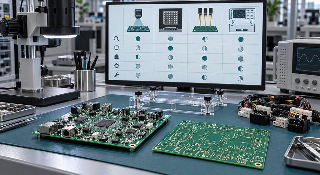
An SMT testing strategy should match likely defects and required functions to suitable inspection and test methods. You also should consider package visibility, electrical access, design maturity, and production volume.
- Define the defects requiring detection.
- Review optical visibility and electrical access.
- Compare methods against production needs.
- Establish functional acceptance requirements.
- Validate the combination during an appropriate build stage.
5.1. Define the Defects That Must Be Detected
Your risk list should identify both the fault and its possible effect. A bridged power rail may prevent safe startup. A missing bypass capacitor may cause intermittent behavior that a simple power-on check misses.
To prioritize these risks effectively, consider conducting design reviews, outlining component requirements, and examining relevant production records. Each significant risk needs a planned check or a documented reason for accepting the gap.
5.2. Review Package Visibility
Package geometry determines which connections optical inspection can evaluate. Hidden terminations, shields, and nearby tall components can block the required view.
Your review should identify these locations before inspection programming begins. If shielding or coating will obscure a connection, the inspection may need to occur earlier. Hidden solder joints may require X-ray imaging selected for the package and defect.
5.3. Review Electrical Test Access
When it comes to electrical testing, a solid connection and accurate measurements is crucial for spotting faults versus acceptable conditions. Just accessible test pads isn’t enough to ensure that reliability. Parallel paths, protective devices, and component tolerances can all influence the outcomes.
Your test developer should identify inaccessible nodes and measurements affected by circuit interactions. From there, the plan can either include an additional check where it makes sense or note any unresolved risks. Plus, it’s important to make sure that any applied stimuli stay within the limits of the devices connected.
5.4. Compare Flying Probe and Fixture-Based ICT
Flying probe often suits PCB prototypes because it avoids a dedicated bed-of-nails fixture. Fixture-based ICT can offer shorter test cycles when the design is stable and repeated production justifies the setup. Actual performance still depends on the board and test program.
When you compared the cost, you should consider program development, fixtures, test time, maintenance, and any expected revisions. Remember, repeat orders are just as important as that initial batch.
5.5. Define Functional Acceptance Requirements
For functional acceptance, it’s essential to have a testable requirement for every behavior you choose to evaluate.
A solid requirement should clearly outline the interface, the test message, the anticipated reply, and the allowable response time.
Additionally, your procedure should also specify firmware, supply conditions, and connected loads. Remember, product specifications should provide the actual limits; they should not be chosen simply to make test results pass.
5.6. Adapt the Plan to the Production Stage
Getting those early builds up and running is crucial for figuring out what can actually be measured and identifying areas where the design could use a bit more accessibility.
Early builds help establish what can be measured and where the design needs better access. When it comes to pilot builds, they should confirm that the production tests are reliable and consistent.
Once we hit stable production, we need to implement controlled programs, keep our fixtures in check, and maintain records that highlight any recurring issues.
The priorities below are planning guidance, not mandatory test combinations.
Build stage | Main planning priority | Evidence needed before progression |
Prototype | Establish test access and investigate design behavior | Recorded findings and coverage gaps to address before the next build |
Pilot or new product introduction | Validate programs, fixtures, limits, and failure handling | Repeatable results and an approved disposition for significant coverage gaps |
Stable production | Maintain approved coverage and production capacity | Controlled revisions, station checks, and traceable test results |
6. FAQ About SMT Testing
Can a PCB Assembly Pass AOI and Still Fail Electrically?
Yes. AOI checks out the visible features as part of its inspection program. However, just because a board passes those checks doesn’t mean it’s flawless; it could still have an incorrect component value, a hidden open connection, or even a damaged device lurking beneath the surface.
Can AOI Replace X-Ray Inspection?
AOI can’t take the place of X-ray when it comes to inspecting hidden solder joints. It can certainly check out the visible parts of a BGA package, like its position or markings, but it won’t be able to see the solder balls underneath.
Does Every SMT Assembly Need Every Test Method?
No. Your test should reflect product risks, available access, production needs, and customer requirements.
7. FAQ About SMT Testing
SMT testing gives you useful acceptance evidence when each check addresses a defined risk or requirement. Physical inspection, electrical measurements, and functional tests answer different questions about the assembly. Even if a test passes under certain conditions, it doesn’t mean all potential defects are gone.
Before you kick off your next build, agree on a written test plan with the assembly supplier. It should identify the checks, acceptance criteria, records, and failure-handling responsibilities. Any remaining coverage gaps need a documented decision before production release.