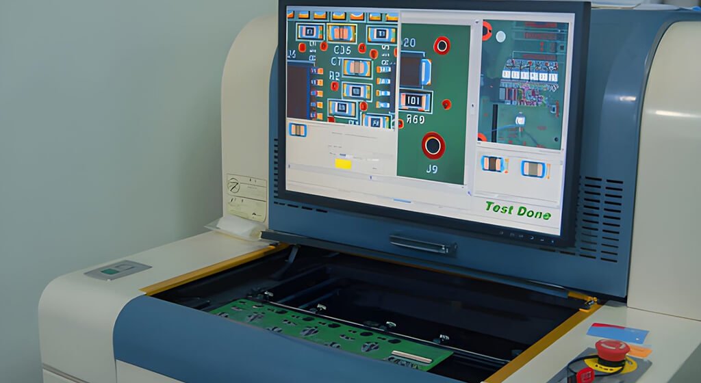
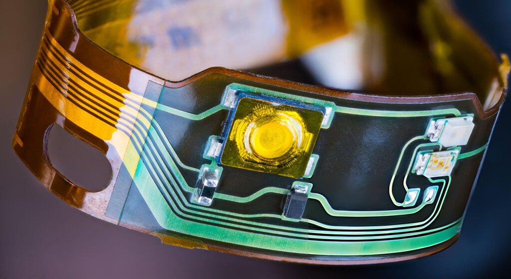
Flex PCB assembly troubleshooting should begin by preserving the failed condition and locating the first process stage where the defect appeared.
Separate possible causes into four domains: bare-board fabrication, surface-mount technology (SMT), mechanical design or handling, and components or testing.
Then confirm the suspected cause with the least destructive evidence available. Rework only after that evidence supports a defined corrective action.
During any investigation, you should follow the procurement drawing, approved material and component documents, solder-paste data, and the standards invoked by the contract. A visible symptom can suggest several causes, but it rarely proves one.
Table of Contents
1. What Is Flex PCB Assembly Troubleshooting?
Flex PCB assembly troubleshooting is a structured failure-isolation process.
It connects an observed symptom to the stage that created it, collects evidence, tests competing explanations, and verifies the corrective action.
It is not simply visual inspection or local repair. A successful investigation also defines how to prevent the same defect from reaching the next production lot.
The investigation should distinguish four failure domains:
- Bare-board fabrication: conductor, via, surface finish, coverlay, lamination, stiffener, dimensional, or cleanliness conditions.
- SMT assembly: support tooling, printing, placement, reflow, cleaning, inspection, or rework conditions.
- Mechanical design and handling: bend geometry, strain concentration, installation path, connector loading, depaneling, or packaging damage.
- Components and testing: package moisture exposure, component cracks, hidden interconnects, test access, or an unsuitable test condition.
These domains can interact. For example, poor carrier support can affect paste registration, placement accuracy, heat transfer, and post-reflow inspection.
The first visible defect may therefore appear later than the condition that created it.
2. Why Is Standard Rigid-PCB Troubleshooting Not Enough?
Rigid-PCB methods is still useful, but they do not cover every flex-specific variable.
A flexible circuit can change shape during printing, placement, heating, cooling, installation, and use.
Thin dielectric layers, localized stiffeners, material movement, moisture history, and bend strain can alter the defect mechanism. They can also change which inspection method provides reliable evidence.
2.1. Low stiffness changes process registration
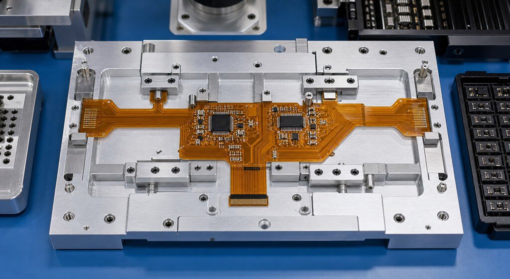
A flex circuit may not stay flat against a stencil or placement support without validated tooling.
Local movement can change stencil contact, paste offset, placement coordinates, and component seating. A rigid, repeatable carrier is common industry practice when the circuit cannot maintain registration by itself.
Carrier selection remains project-specific.
Tooling holes, fiducials, component access, vacuum paths, tape or adhesive compatibility, heat transfer, cleaning, and release all affect the result.
The carrier must support the assembly without contaminating solderable surfaces or loading a bend-sensitive area.
2.2. Thin material systems make heat and force more consequential
Repeated heating or mechanical pulling can damage copper adhesion, coverlay, dielectric, pads, and stiffener transitions. A repair that looks acceptable under a microscope may still have reduced mechanical margin.
This risk is higher when the repaired region will bend during installation or operation.
Material datasheets help engineers compare properties, but they do not set finished-assembly limits. Qnity’s Pyralux laminate product information describes named material systems for flex and rigid-flex construction.
Use the current data sheet for the selected product when comparing properties and test conditions. Those values cannot predict flex-PCBA life without the actual stackup, copper geometry, assembly process, and use condition.
2.3. The assembly keeps moving after soldering
A static continuity test may pass while a conductor opens at one installed angle. Solder joints, vias, traces, components, and stiffener edges can experience strain after final assembly.
Troubleshooting must therefore include the real installation path and operating motion when those conditions are relevant.
Our flex PCB materials guide provides background on base films, copper, adhesives, coverlay, and stiffeners. Use that material context to frame questions, then confirm the selected product data with the actual supplier documentation.
Do You Need Any Help?
3. Which Flex PCB Defects Should You Check First?
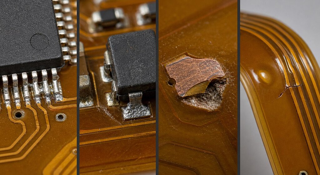
Start with the observed symptom, not a favorite root-cause theory.
Record when and where the condition appeared, then collect evidence that can separate plausible causes.
The table below identifies useful first checks. Its “likely domain” column narrows the search; it does not assign final responsibility or replace the applicable acceptance criteria.
Observed Symptom | Likely Failure Domain | Evidence To Collect | First Safe Action | Confirmation Method |
Paste Is Missing, Smeared, Or Offset | Tooling or printing | Carrier position, underside condition, stencil record, solder paste inspection (SPI) data | Stop the printer and preserve an unpopulated sample | SPI trend, stencil inspection, registration study |
Component Is Shifted Or Rotated | Printing, placement, or tooling | Post-print SPI, post-place image, placement logs, fiducial results | Hold the affected panel before reflow if possible | Compare pre-reflow and post-reflow positions |
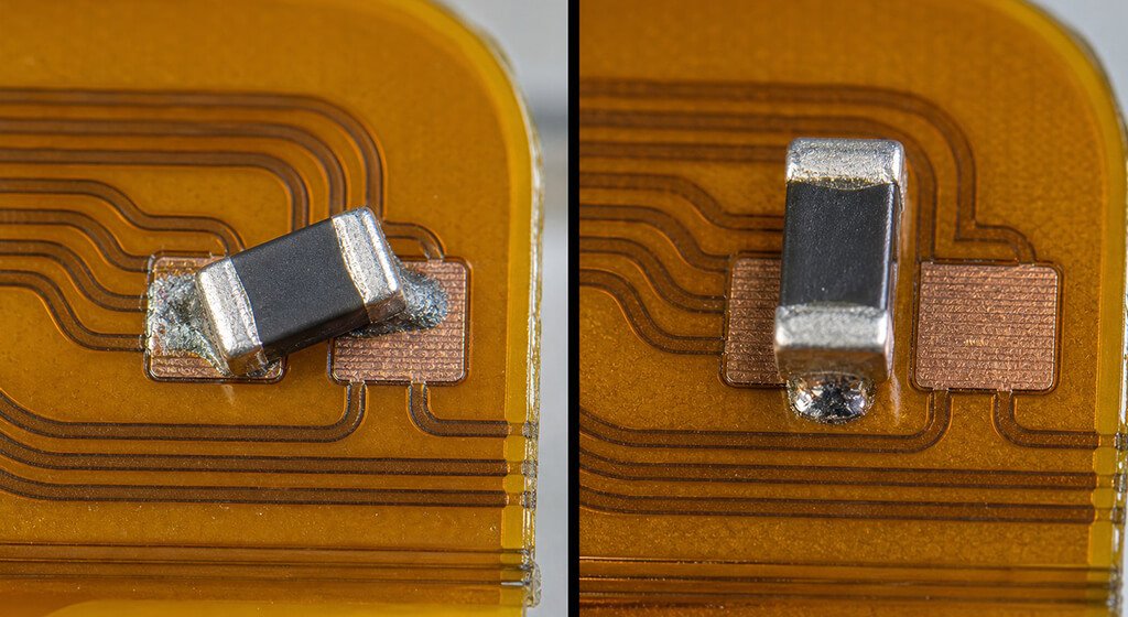
One End Of A Chip Stands Upright | Printing, placement, thermal balance, or land design | Paste volume at both ends, placement height, copper connections, joint temperatures | Contain the lot and retain paired deposits | SPI, automated optical inspection (AOI), product profile |
Joint Is Dull, Nonwetted, Or Electrically Open | Surface condition, paste, component, or reflow | Finish and storage history, paste record, component termination, measured profile | Avoid reheating the only failed sample | Microscopy, solderability evidence, electrical test, microsection if justified |
Bridge Or Solder Ball Appears After Reflow | Printing, placement, paste handling, or thermal process | Pre-reflow paste result, placement pressure, paste exposure, post-reflow image | Preserve the deposit-to-joint evidence chain | Correlate SPI, placement data, and AOI or X-ray |
Pad Lifts Or Coverlay Discolors | Reflow, rework, bare-board construction, or handling | Heat-cycle history, tool settings, photographs, trace condition, material record | Stop further heat and mechanical force | Microscopy, continuity, peel/interface review, microsection |
Bubble, Blister, Or Internal Separation Appears | Moisture, lamination, contamination, or excess heat | Packaging and exposure history, incoming photos, material lot, product temperatures | Quarantine affected material before another heat cycle | X-ray where suitable, microscopy, destructive microsection |
Board Buckles Or Loses Registration | Incoming shape, carrier, copper balance, or thermal gradient | Flatness before and after loading, reflow, cooling, and release | Hold the carrier and affected panel for comparison | Dimensional |
4. How Should You Troubleshoot a Flex PCB Assembly?
Use an evidence-first sequence: contain the material, preserve the failed state, identify when the defect first appeared, classify the suspected domain, and choose a suitable confirmation method.
Compare failed and known-good samples before changing the process. After correction, verify both defect removal and process stability. Random rework can destroy evidence and create a second failure mechanism.
4.1. Contain the affected material
Stop shipment or downstream processing for the defined lot, panel position, machine window, or time period.
Keep traceability to the flex bare-board lot, paste batch, component date code, carrier, stencil, line, oven recipe, operator, and inspection program where those records exist.
Containment should be narrow enough to remain useful and broad enough to protect the customer.
Do not assume every board in the lot has the same failure mode. Sampling and disposition must follow the project’s risk and contractual requirements.
4.2. Preserve the failed condition
Photograph the assembly before cleaning, probing, bending, heating, scraping, or component removal. Record the reference designator, X-Y location, panel position, orientation, inspection stage, and test signature. Save representative failures as well as known-good controls.
Do not reflow the only failed sample to “see whether it improves.”
Heat can change wetting evidence, close an intermittent crack, worsen delamination, or damage a component.
If destructive analysis may be needed, preserve all available nondestructive records first.
4.3. Locate the first stage where the defect appears
Compare evidence from incoming inspection, post-print SPI, post-placement inspection, post-reflow inspection, electrical test, depaneling, installation, and field use.
The first stage showing the abnormal condition usually narrows the responsible process more effectively than the final symptom alone.
A component that is correct after placement but shifted after reflow points away from coordinate programming.
An open that appears only after housing installation points toward mechanical loading, although the weakened feature may have originated earlier.
4.4. Test competing explanations
List two or three plausible mechanisms and identify evidence that would separate them.
For a nonwetted joint, compare surface condition, paste history, component termination, temperature data, and neighboring joints.
For an intermittent open, compare the electrical signature at rest and during controlled movement.
Start with nondestructive methods when they can answer the question. Escalate to cross-sectioning or component removal only after the evidence value exceeds the cost of losing the specimen.
4.5. Correct, verify, and prevent recurrence
Separate immediate correction from preventive action. Removing a bridge corrects one assembly; stabilizing the print process prevents recurrence. Verify the change through first-article evidence, controlled trial builds, process data, and the required inspection or test.
Document the confirmed root cause, affected scope, correction, owner, verification result, and control-plan change. If the mechanism remains unproven, label it as a suspected cause rather than closing the investigation prematurely.
The IPC-9111 troubleshooting guide provides assembly symptom-cause-action relationships. Flex-specific conclusions still need evidence from the circuit construction, carrier, thermal history, and mechanical use.
Do You Need Any Help?
5. Where Do Flex Assembly Failures Begin?
Flex assembly failures can begin before printing, during SMT processing, or after the board leaves the line. Map each symptom to the earliest stage that could have created it.
Every stage has evidence that can be collected or destroyed. A useful control plan therefore defines records at incoming inspection, printing, placement, reflow, inspection, handling, installation, and test.
5.1. Incoming flex circuits, components, and solder paste
Check packaging condition, humidity indicator card where used, desiccant, exposure records, surface finish, flatness, dimensions, tooling features, contamination, and electrical test status. Match the board construction to the released drawing and material specification.
Keep bare-board moisture control separate from component Moisture Sensitivity Level (MSL) control. IPC-1602A addresses printed-board handling and storage. J-STD-020F and J-STD-033D address moisture/reflow-sensitive components.
Do not apply one automatic bake schedule to every flex board. The decision needs the material system, construction, packaging, exposure history, solderability risk, board-supplier guidance, and a validated project procedure.
5.2. Carrier loading and panel support
Record the carrier identity, loading method, locating features, support surfaces, and any tape, adhesive, vacuum, clamp, or cover-plate use.
Confirm that critical pads remain flat and fiducials remain visible. Check for residue, wear, distortion, and repeatability after thermal cycling and cleaning.
Measure the circuit before loading, while restrained, after reflow, and after release when warpage is under investigation.
Those observations help separate incoming shape, fixture-induced strain, temporary thermal movement, and permanent deformation.
5.3. Solder-paste printing and SPI
Printing evidence includes paste volume, height, area, shape, and offset.
Review the stencil revision, aperture condition, underside cleaning, paste temperature and working time, squeegee settings, separation, and support below critical land patterns.
Three-dimensional SPI can quantify deposits before placement and reflow. It cannot assess the finished solder joint.
Our AOI and inspection guide explains why inspection coverage must match the defect and production stage.
5.3. Placement and machine records
Retain placement coordinates, fiducial results, pickup errors, nozzle selection, Z-height, placement force where available, and post-placement images.
Compare the position before and after reflow. That comparison separates placement error from later movement caused by solder forces or thermal imbalance.
5.4. Reflow and product-temperature evidence
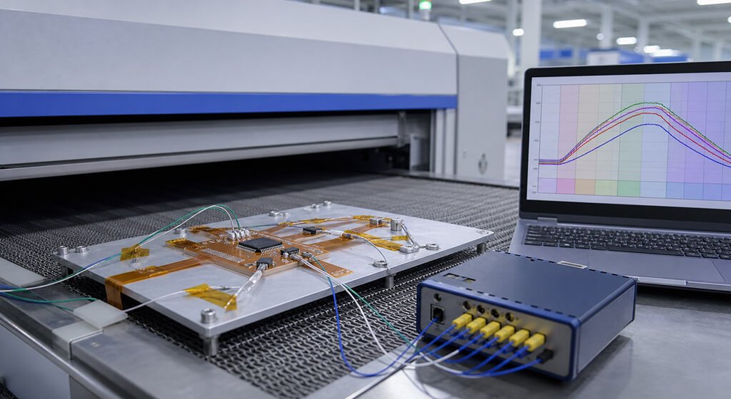
Oven zone settings describe the machine recipe, not the temperatures reached at each solder joint. Use properly attached, calibrated thermocouples on a production-representative assembly. Place them at thermal extremes and relevant failure locations.
IPC-7530B provides profiling guidance, while IPC-7801A addresses reflow-oven process control.
Measurement traceability should connect the recorded result to a documented calibration chain. NIST explains that traceability is a property of a measurement result, not a label automatically attached to an instrument.
5.5. Handling, depaneling, installation, and use
Record when the assembly first sees unsupported lifting, connector insertion, folding, depaneling force, coating, cleaning, packaging pressure, housing installation, vibration, or repeated movement.
Reproduce the real condition only within the approved mechanical and electrical test envelope.
6. What Are the Common Flex PCB Assembly Defects and Fixes?
Common flexible PCB assembly defects include print variation, bridges, component movement, tombstoning, nonwetting, pad lift, delamination, warpage, and intermittent opens. The corrective action depends on the verified mechanism.
For each defect, compare evidence before and after the stage where it appeared. Repair the affected unit only after containment protects the remaining lot.
6.1. Defect, Cause, Detection, and Prevention Matrix
Use this matrix to compare failure mechanisms before choosing a corrective action. It summarizes the strongest differentiating evidence and the control most likely to prevent recurrence.
Final acceptance and disposition still depend on the invoked standard, product risk, and verified project data.
Defect Or Symptom | Plausible Causes | Detection Or Differentiating Evidence | Prevention After Confirmation |
Insufficient Paste Or Bridging | Poor aperture release, stencil gap, excess deposit, circuit movement, paste condition | SPI trend, stencil inspection, fiducial-to-deposit offset, panel-position pattern | Stabilize support, control stencil condition and paste handling, validate aperture changes with SPI |
Component Shift Or Tombstoning | Unequal paste, placement error, high force, carrier motion, land or thermal imbalance | Compare post-place and post-reflow images, paired SPI deposits, placement log, product profile | Improve carrier repeatability, balance deposits and lands, control placement, verify the thermal window |
Nonwetting Or Open Joint | Oxidation, contamination, weak flux activity, insufficient heat, termination condition | Microscopy, storage and paste history, thermocouple data, electrical and solderability evidence | Protect solderable surfaces, control material exposure, and validate the overlapping paste, component, and board window |
Lifted Pad Or Coverlay Damage | Cumulative heat, long dwell, mechanical force, weak adhesion, unsupported rework | Heat-cycle history, tool settings, microscopy, continuity, microsection when justified | Set a rework stop rule, support the flex, control temperature and force, require MRB approval when structure is affected |
Delamination Or Blistering | Moisture, weak lamination, contamination, incompatible materials, excess thermal exposure | Packaging and exposure history, incoming images, product profile, X-ray where suitable, microsection | Use dry handling, validate any bake decision, control lamination and materials, prevent unnecessary heat cycles |
Warpage Or Buckling | Incomplete support, carrier distortion, copper imbalance, stiffener geometry, thermal gradient | Flatness before loading, during restraint, after reflow, after cooling and release | Correct support and datum strategy, review copper and stiffener balance, reprofile after tooling changes |
Intermittent Open During Bending | Cracked copper, via damage, solder fracture, cracked component, installation strain | Controlled bend-resistance trace, position correlation, microscopy, X-ray, targeted microsection | Redesign the bend or stiffener transition, control installation, and qualify the actual motion envelope |
6.2. Insufficient paste, bridging, and print inconsistency
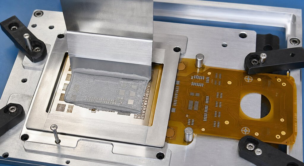
Symptom: Paste deposits are incomplete, offset, smeared, or connected across adjacent pads. After reflow, joints may be open, solder-starved, bridged, or surrounded by solder balls.
Plausible causes: Poor aperture release, a stencil-to-board gap, circuit movement, incorrect alignment, worn apertures, contamination, paste outside its approved working condition, or unstable separation can create the pattern. Excessive placement pressure or paste slump may turn an acceptable print into a post-reflow bridge.
Differentiating evidence: Compare SPI results by panel position and against the carrier coordinate system. A consistent offset suggests registration error. Random variation suggests movement, poor support, contamination, or unstable printing.
Correction and prevention: Clean or repair the stencil, stabilize local support, correct registration, and validate any aperture or process change with measured deposit data. Do not copy one aperture-reduction percentage across unrelated packages, paste products, and stencil technologies. IPC-7525C provides stencil design guidance, while IPC-7527 addresses solder-paste printing requirements.
6.3. Component shift, rotation, and tombstoning
Symptom: A component moves outside its intended lands, rotates, skews, or rises on one end during reflow.
Plausible causes: Unequal paste volume, placement error, high placement force, circuit movement, land asymmetry, different copper heat sinking, termination condition, or unequal wetting can generate unbalanced forces.
Differentiating evidence: Compare post-place and post-reflow images. Review the two paste deposits, placement height, pad geometry, copper connections, component terminations, and measured temperatures. If the component was centered before reflow, coordinate correction alone will not solve the mechanism.
Correction and prevention: Correct the confirmed imbalance in support, printing, placement, land design, or thermal process. Verify the change across relevant panel positions and repeated carrier cycles.
Do You Need Any Help?
6.4. Nonwetting, cold or disturbed joints, and void concerns
Symptom: The joint does not wet the land or termination, has an irregular disturbed surface, opens electrically, or shows an unacceptable hidden-solder condition under the project criteria.
Plausible causes: Surface oxidation, contamination, damaged finish, expired or mishandled paste, insufficient flux activity, inadequate temperature, movement during solidification, component termination problems, or an unsuitable atmosphere can contribute.
Differentiating evidence: Review board and component storage, paste history, surface condition, measured joint temperatures, neighboring joints, and solderability results where justified. Visual appearance alone cannot prove metallurgical integrity or long-term reliability.
Correction and prevention: Protect solderable surfaces, control material exposure, and establish an overlapping process window for paste, components, and the flex construction. Verify temperatures on the product. Use electrical or destructive analysis when visual evidence cannot answer the root-cause question.
The following numbers are our specific example, not a universal flex PCB reflow profile:
Parameter | Indium RMA-155 SAC305 Starting Guidance |
Average Ramp Rate From Ambient To Peak | 1.0–1.5°C/s |
Optional Soak | 140–160°C for 20–60 seconds |
Time Above Liquidus | 45–60 seconds |
Peak Temperature | 230–260°C |
Cooling Rate | 2–6°C/s |
Atmosphere | Air or nitrogen |
6.5. Lifted pads, coverlay damage, and heat damage
Symptom: A copper pad moves, the attached trace peels, coverlay discolors, the dielectric tears, or the local surface chars during reflow or rework.
Plausible causes: Excessive temperature, long dwell, cumulative heat exposure, mechanical pulling, unsupported rework, weak adhesion, construction damage, or unsuitable removal tools can cause the condition.
Differentiating evidence: Preserve the heat-cycle history, tool settings, photographs, and component-removal sequence. Inspect the attached conductor, nearby coverlay, via connections, remaining adhesion, and signs of damage below the visible surface.
Correction and prevention: Stop heat and force as soon as structural movement appears. A Material Review Board (MRB) or other authorized team should decide whether repair is permitted. The decision must consider the governing class, customer authorization, inspection access, and future flexing.
6.6. Delamination and reflow-related separation
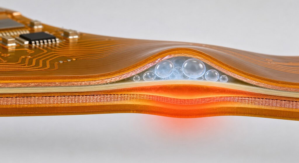
Symptom: Bubbles, blisters, coverlay separation, or internal interface gaps appear during or after thermal processing.
Plausible causes: Moisture can contribute, but it is not the only explanation. Weak lamination, contamination, incompatible materials, excessive temperature, long exposure, trapped volatiles, or fabrication damage can produce similar symptoms.
Differentiating evidence: Compare incoming images, packaging and exposure records, material lot data, lamination records, and product temperatures. X-ray may reveal some internal geometry, but microsectioning may be needed to confirm the physical interface. A cross-section destroys the selected sample.
Correction and prevention: Quarantine affected material before another heat cycle. Confirm the failure mechanism before adding a bake step. Dry handling, validated storage, supplier controls, and a project-specific drying decision provide stronger prevention than universal baking
6.7. Warpage, buckling, and carrier-related distortion
Symptom: The flex circuit curves, wrinkles, lifts from the carrier, or loses print and placement registration.
Plausible causes: Incomplete support, carrier distortion, copper imbalance, stiffener geometry, material movement, adhesive behavior, heavy components, or temperature gradients can change shape.
Differentiating evidence: Measure flatness before heating, after loading, after reflow, after cooling, and after release. Map distortion against copper, stiffeners, component mass, carrier support, and oven direction.
Correction and prevention: Modify the support scheme only after the measurements identify where restraint is missing or harmful. Reprofile the product after a carrier change because support and thermal mass can alter joint temperatures.
6.8. Cracked copper and intermittent opens
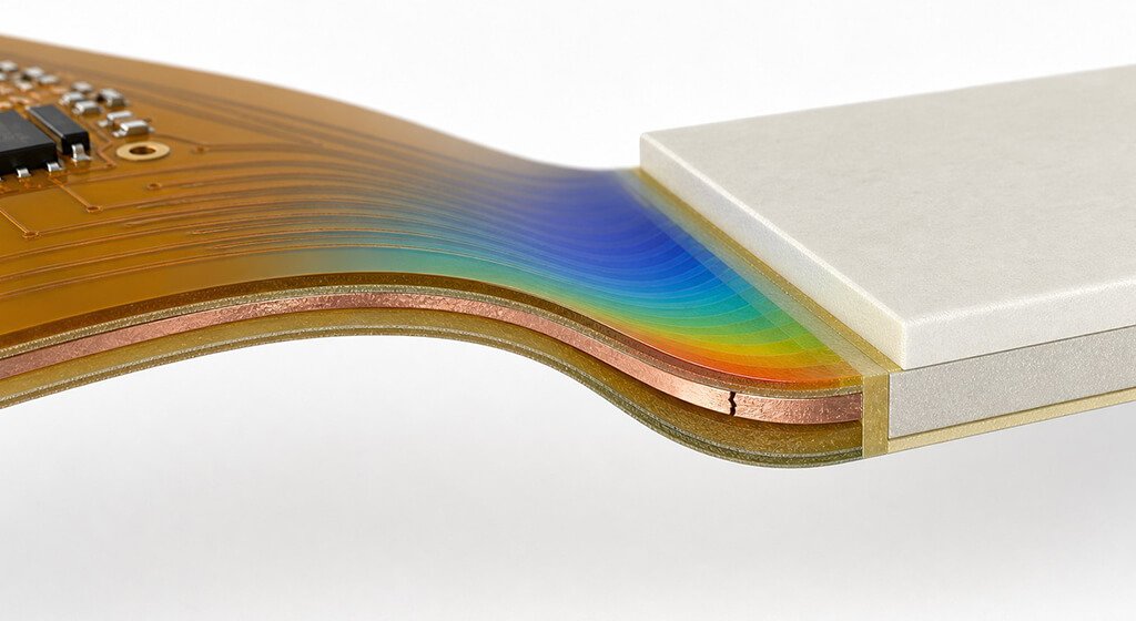
Symptom: The assembly passes at rest but opens during folding, vibration, thermal change, connector loading, or installation.
Plausible causes: A small bend radius, repeated motion, a via, a sharp corner, stacked traces, a narrow neck-down, or a stiffener edge can concentrate strain in the flex. Installation damage, a cracked component, or a solder-joint fracture can create the same electrical signature.
Differentiating evidence: Monitor continuity or resistance while applying a controlled radius, angle, direction, and rate. Correlate the electrical event with video or position data. Microscopy, X-ray, four-wire measurements, or a later microsection can then localize the feature.
Correction and prevention: Do not prescribe one bend-radius multiplier without the construction and use requirements. Review copper type, thickness, layer count, trace direction, bend cycles, temperature, coverlay, and stiffener transition. IPC-2223F supports flex and rigid-flex design review, while the project drawing and qualification plan must define the actual use case.
Do You Need Any Help?
7. Which Design and Process Parameters Matter Most?
The most important parameters are those that control circuit position, paste transfer, component seating, thermal exposure, material condition, and installed strain.
Their limits are not universal. Define them from the released stackup, BOM, assembly drawing, material and paste documents, equipment capability, end-use motion, reliability target, and standards invoked by the purchase agreement.
Parameter Or Decision | Evidence Needed | Why It Matters | Decision Owner |
Static, Installation-Flex, Or Dynamic Use | Product motion, cycle target, bend geometry, drawing | Changes conductor design, test method, and disposition risk | Product and flex-design engineering |
Bend Location And Radius | Full stackup, copper, coverlay, stiffener, motion, qualification | Controls conductor and interface strain | Product engineering with board supplier |
Carrier And Support Method | Geometry, datums, panel, component sides, thermal study | Controls flatness, registration, placement, and heat transfer | Manufacturing engineering |
Stencil And Aperture Design | Land pattern, paste, stencil technology, SPI capability | Controls deposit volume and release | SMT process engineering |
Placement Force And Height | Package, nozzle, support, paste tack, machine data | Can bend the flex or displace paste | SMT process engineering |
Bare-Board Moisture Plan | Construction, packaging, exposure, HIC, supplier guidance | Balances delamination and solderability risks | Board supplier and process engineering |
Component MSL Control | Part number, label, floor-life log, package guidance | Protects moisture-sensitive devices from reflow damage | Materials and process engineering |
Reflow Process Window | Paste, component limits, material system, carrier, measured profile | Controls wetting without exceeding product limits | SMT process engineering |
Inspection Coverage | Package list, hidden joints, risk, volume, records needed | Determines which defects can be detected and contained | Quality and test engineering |
Rework Stop Rule | Heat history, structure, accessibility, class, customer approval | Prevents repair attempts from creating structural damage | MRB or authorized customer team |
7.1. Choose standards by function
Different standards address different objects. IPC-6013E covers flexible and rigid-flex bare-board qualification and performance. It is not a completed-assembly solder-joint acceptance standard.
IPC J-STD-001J covers soldered assembly materials and process requirements. IPC-A-610J addresses completed assembly acceptability when the relevant class and requirements are invoked. Neither standard, by itself, proves field life.
Contracts may call out an earlier revision or an industry addendum. Record the applicable revision, class, addenda, and order of precedence before production. Never assume that “IPC Class 3” means zero defects or guarantees reliability in a specific environment.
7.2. Review design and manufacturing together
Keep components, vias, sharp conductor transitions, and abrupt stiffness changes away from dynamic bend areas when the electrical and mechanical design permits. Use smooth trace routing, suitable pad support, controlled coverlay openings, and strain relief at stiffener transitions.
Review panelization, tooling holes, fiducials, carrier access, component zones, and installation drawings before fabrication.
Do You Need Any Help?
8. Which Inspection and Failure-Analysis Method Should You Use?
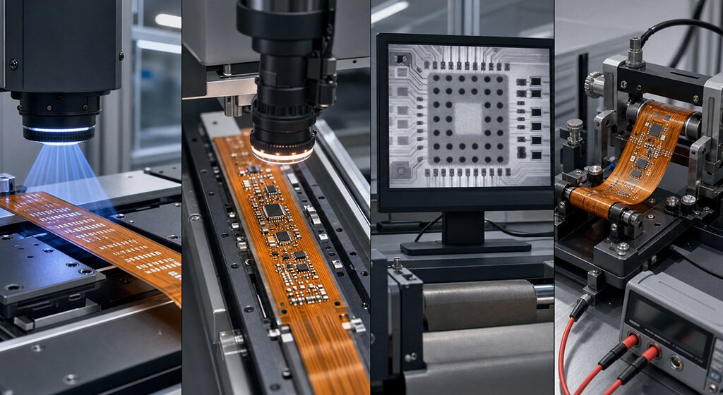
Choose the method that can observe the suspected feature at the correct production stage. SPI, AOI, X-ray, electrical test, controlled bending, microscopy, and microsectioning answer different questions.
A positive result can support one mechanism without excluding every alternative. Record each method’s resolution, program, calibration, sample condition, and known detection limits.
Method | Best For | What It Does Not Prove | Sample Impact | Best Decision Point |
3D SPI | Paste volume, height, area, shape, and offset | Final solder-joint quality | Nondestructive | Before placement and reflow |
Post-Place AOI | Presence, polarity, rotation, and visible position | Movement that occurs later in reflow | Nondestructive | Before reflow when accessible |
Post-Reflow AOI | Visible bridges, position, polarity, and surface features | Hidden joints, electrical function, or metallurgy | Nondestructive | Production screening and trend control |
X-Ray | Hidden solder geometry, bridges, voids, alignment, some opens | Every cold joint, every interface crack, or electrical performance | Usually nondestructive | Hidden-joint investigation and screening |
Electrical Continuity Or Resistance | Opens, shorts, and resistance change | Physical location or dynamic durability | Nondestructive if limits are safe | Bare-board, assembly, and failure analysis |
Functional Test | Product behavior under defined inputs and loads | Exact physical root cause | Usually nondestructive | Final test and failure reproduction |
Controlled Bend Continuity | Position-dependent intermittent opens | Service life outside the defined test envelope | Can add fatigue if uncontrolled | Mechanical failure isolation |
Optical Microscopy | Surface cracks, lifted features, contamination, visible workmanship | Hidden interfaces or internal copper | Nondestructive at normal inspection levels | Triage and localized analysis |
Microsection | Internal copper, via, pad, plating, and interface damage | Conditions elsewhere in the lot without sampling support | Destructive | Final physical confirmation |
9. When Should You Rework, Scrap, or Escalate a Flex Assembly?
Rework is reasonable only when the defect is accessible, the surrounding structure remains sound, and an approved procedure can restore the required condition.
Scrap or engineering escalation becomes more appropriate when conductors, pads, coverlay, dielectric, vias, or dynamic bend regions are damaged.
Cumulative heat exposure, product class, test access, and customer authorization must guide the decision.
9.1. Consider controlled rework
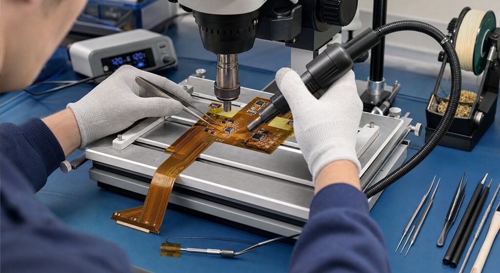
A limited bridge, accessible solder deficiency, misplaced replaceable component, or local contamination may support controlled rework. Confirm that pads, traces, coverlay, substrate, nearby components, and stiffener interfaces remain intact.
Use defined tools, local support, suitable flux, temperature control, shielding, magnification, and post-rework inspection. Document the procedure and cumulative thermal history. IPC-7711/21D provides recognized rework, modification, and repair procedures, but it does not automatically authorize repair for every product.
9.2. Stop and escalate
Stop when a pad moves, a conductor peels, the dielectric tears, coverlay separates, the surface chars, or the approved thermal limit may be exceeded.
Also stop when the repair cannot be inspected adequately or when customer requirements demand MRB approval.
Dynamic bend-area damage deserves special caution. A local jumper or adhesive repair can create a new stiffness transition.
A restored static continuity result does not prove that the repaired assembly will meet its required motion life.
9.3. Consider scrap
Severe or spreading delamination, carbonization, torn dielectric, widespread pad lifting, inaccessible conductor damage, and repeated thermal abuse often favor scrap. High-reliability and regulated products may have stricter disposition rules.
Record the final decision as repair, use-as-is, return, or scrap. Link it to defect images, analysis evidence, approval, verification, and the affected production lot.
Do You Need Any Help?
10. How Do Application Requirements Change the Investigation?
The same visible defect can require different evidence and disposition in a static consumer product, a dynamic wearable, a rigid-flex control module, or a regulated device.
Define the mission, movement, environment, service life, electrical risk, and acceptance documents before selecting tests. A troubleshooting result is valid only within the conditions that were evaluated.
10.1. Static and installation-flex circuits
A static flex may bend only during installation and then remain fixed. Troubleshooting should still reproduce the installation path, connector loading, and final restraint. An installation bend can damage copper even if the product has no repeated operating motion.
10.2. Dynamic flex circuits
Dynamic applications need a defined radius, axis, angle, travel, rate, cycle target, electrical load, temperature, and failure threshold. A single hand-bend test provides weak evidence and may add damage. The validation plan should represent the intended service condition and its uncertainty.
10.3. Rigid-flex and high-density assemblies
Rigid-flex products combine flex-region mechanics with rigid-section SMT behavior. Stiffness transitions, plated structures, buried interfaces, and hidden packages may require several inspection methods.
Our turnkey PCBA service can coordinate fabrication, sourcing, assembly, and test, but the project still needs an agreed evidence and acceptance plan.
10.4. High-reliability or regulated products
Medical, automotive, aerospace, industrial safety, and other high-consequence products often require formal change control, traceability, qualification, and customer approval.
An ISO 9001 certificate describes a quality-management system; it does not set flex-defect limits or prove the reliability of one assembly. UL material or construction recognition also does not replace product-level reliability validation.
11. What Should Engineers Send for Failure Analysis?
A useful supplier handoff package should identify the product, failed condition, process history, and decision required.
Send controlled design files and measured evidence rather than a defect photo alone. State whether the goal is lot containment, root-cause confirmation, rework disposition, DFM correction, or a preventive process change. Remove customer-confidential information only through an agreed process.
Use this checklist before escalation:
- Released Gerber or ODB++ data, fabrication drawing, assembly drawing, and panel data.
- Stackup, material system, copper type and thickness, coverlay, stiffener, and surface finish.
- Bill of materials (BOM), component labels, approved-vendor information, and relevant package documents.
- Component placement list (CPL), centroid data, fiducials, and polarity information.
- Defect photographs with reference designator, X-Y location, panel position, orientation, and scale.
- Failed quantity, lot quantity, date range, machine or line, and inspection stage.
- Incoming, SPI, post-place, AOI, X-ray, electrical, and functional records that exist.
- Reflow recipe and product thermocouple profile, including attachment and calibration information.
- Bare-board packaging and exposure history, plus component MSL exposure records.
- Depaneling, cleaning, coating, connector insertion, installation, bend, and rework history.
- Known-good comparison samples and representative unreworked failures.
- Applicable IPC revision, class, addendum, customer specification, and required disposition deadline.
12. How Can PCBSAIL Support a Flex PCB Troubleshooting Project?
We can support a flex troubleshooting project by combining its publicly documented flex fabrication, assembly, SMT, sourcing, inspection, and electrical-test services within a project-specific scope.
The main risks are circuit movement, print and placement variation, thermal exposure, hidden joints, and electrical failures.
The quotation should define the selected methods, coverage, records, and responsibility for every requested output.
12.1. What Files Should You Send Us?
For a quotation and design for manufacturability (DFM) review, provide:
- Gerber files or ODB++ data.
- Bill of materials (BOM) with manufacturer part numbers and approved alternates.
- Pick-and-place or centroid data.
- Fabrication, assembly, panel, and mechanical drawings.
- Stackup, material, coverlay, stiffener, surface-finish, and IPC requirements.
- Electrical, functional, programming, inspection, and reporting requirements.
For an active troubleshooting case, also provide:
- Defect photographs and a reference-designator or X-Y location map.
- Failed quantity, lot quantity, panel position, and the first stage where the defect appeared.
- Available SPI, AOI, X-ray, electrical, and functional-test records.
- Reflow recipe and measured product thermocouple profile.
- Bare-board packaging history and component MSL exposure records.
- Installation, bending, cleaning, coating, handling, and rework history.
- Known-good samples and representative failures that have not been reworked.
Do You Need Any Help?
13. FAQ About Flex PCB Assembly Troubleshooting?
Why do components move more easily during flex PCB reflow?
Flex circuits can move because they have low bending stiffness and may not stay registered without suitable support. Unequal paste deposits, placement pressure, land geometry, copper distribution, and thermal gradients can add unbalanced forces. Compare post-placement and post-reflow positions, then verify carrier stability, SPI data, and measured joint temperatures before changing coordinates.
How can I distinguish a cracked trace from a bad solder joint?
Monitor continuity or resistance while applying a controlled, documented bend condition. A position-dependent event suggests a mechanical fault, but it does not locate the feature by itself. Correlate the electrical signature with microscopy, X-ray, component checks, and installation geometry. Use microsectioning only after nondestructive evidence has been preserved.
Can a delaminated flex PCB be reworked safely?
Do not assume delamination is safely repairable. Quarantine the assembly and determine the separation location, extent, cause, and thermal history. Rework may worsen an internal interface or hide evidence. The authorized MRB or customer should decide disposition using the applicable requirements, inspection access, end-use risk, and a documented repair procedure.
When is X-ray useful for flex PCB assembly defects?
X-ray is useful for hidden solder geometry, bridges, voids, alignment, and some opens under packages such as BGAs and QFNs. Detection depends on resolution, viewing angle, package structure, program, and validation. X-ray does not prove every cold joint, copper crack, or electrical failure, so combine it with electrical and other physical evidence.
Should flex PCBs be baked before assembly?
Not automatically. Bare-board handling belongs under IPC-1602A and the board supplier’s documentation, while component MSL control belongs under J-STD-020F and J-STD-033D. Decide from the actual construction, packaging, exposure, solderability risk, and validated procedure. Unnecessary baking can consume process time and may reduce solderability or add handling risk.
How should a flex PCB be supported during printing and reflow?
Use a repeatable carrier or support method when the flex cannot remain flat and registered by itself. The design must account for datums, fiducials, component access, vacuum or restraint, contamination, release, and heat transfer. Validate printing, placement, product temperatures, and carrier stability across repeated production cycles.
References
– [IPC-2223F]— sectional design standard for flexible and rigid-flex printed boards.
– [IPC-6013E]— qualification and performance specification for flexible and rigid-flex bare boards.
– [IPC-1602A] — printed-board handling and storage.
– [IPC-9111]— troubleshooting relationships for printed-board assembly processes.
– [IPC J-STD-001J] and [IPC-A-610J]— soldered-assembly process requirements and completed-assembly acceptability.
– [IPC-7530B] and IPC-7801A — product profiling guidance and reflow-oven process control.
– [IPC-7711/21D]— rework, modification, and repair procedures.
– [IPC-9716A] and IPC-9242 — automated inspection process control and microsection evaluation.
– [IPC/JEDEC J-STD-020F] and [J-STD-033D — component moisture/reflow sensitivity and handling.
– [NIST metrological traceability guidance]— measurement traceability and calibration-chain principles.
– [Qnity Pyralux laminate product information] — named flex-material context; obtain the current product data sheet before using property values.
– [Indium RMA-155 solder paste data sheet] — supplier-specific paste handling, printing, and reflow guidance used in the example.