
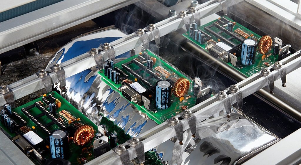
Wave soldering is a mass-soldering process in which a fluxed and preheated printed circuit board assembly passes over a controlled wave of molten solder.
It forms many accessible joints during one conveyor pass and is used mainly for through-hole technology (THT) assemblies and compatible mixed-technology boards.
Reliable wave soldering depends on the measured response of the actual assembly, not one universal pot temperature or contact time. Board thickness, copper planes, component finishes, flux, alloy, fixtures, and equipment settings all influence the final solder joints.
In this article, we will deep into wave soldering process control, profiling, defects, PCB design, and so on.
Table of Contents
1. What Is Wave Soldering?
Wave soldering is a continuous assembly process in which the solder side of a PCB contacts a pumped wave of molten solder.
Flux and preheat prepare the surfaces before contact. The process normally serves through-hole joints, but approved bottom-side surface-mount devices may also be soldered when their packages, footprints, adhesive, and thermal limits permit it.
PCB board is not immersed indiscriminately in a solder pot. A conveyor controls its angle and speed. The solder module controls wave shape, flow, height, and contact length. Preheat and flux settings prepare the assembly for that brief contact.
1.1. What Types of PCB Assemblies Use Wave Soldering?
Wave soldering is a strong candidate when a design contains many through-hole connectors, transformers, relays, switches, or other leaded components. It is most attractive when the solder side is accessible and the product runs often enough to justify profiling, fixtures, and setup.
Mixed-technology boards can also use the process. Surface-mount technology (SMT) parts are normally reflow soldered first. Compatible through-hole parts are inserted afterward, then the assembly crosses the wave.
Some designs place small SMDs on the bottom side and secure them with adhesive before wave soldering. That route requires package-specific approval. For example, Texas Instruments publishes wave-exposure guidance for selected SMT packages. A result for one package cannot authorize an unrelated package.
1.2. What the Solder Wave Does at a Plated Through-Hole?
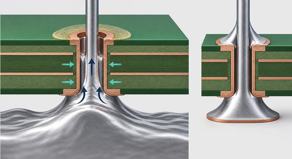
Flux removes or disrupts surface oxides during heating. When the board contacts the solder wave, molten alloy wets the exposed land, barrel, and component lead. Capillary action and pressure from the wave help solder move upward through the plated through-hole (PTH).
The joint starts to solidify after it separates from the wave. Drainage and separation behavior affect the final fillet, solder volume, and risk of bridging. The solder-pot setpoint does not describe this full event. Temperatures at the barrel, top-side land, lead, board surface, and component body can differ substantially.
2. How Does the Wave Soldering Process Work?
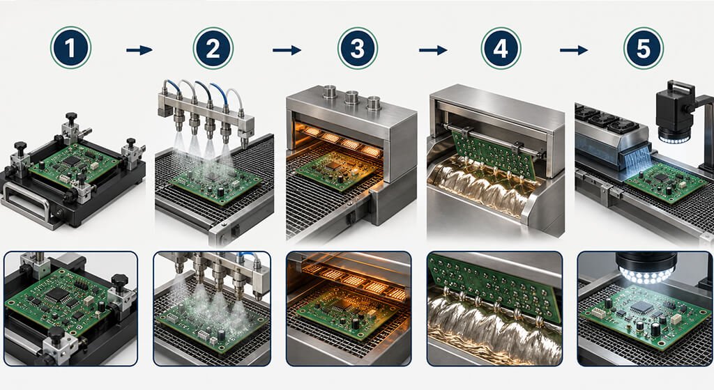
A controlled wave soldering process has five linked stages: preparation, flux application, preheating, solder contact, and post-solder handling. Each stage prepares the next one.
A defect seen after soldering may originate in PCB storage, component solderability, fixture design, flux coverage, or heat transfer rather than in the solder wave itself.
Process Stage | Engineering Objective | Controlled Inputs | Evidence to Retain | Common Risk |
Preparation | Present clean, solderable, correctly positioned features | Material identity, storage, lead forming, insertion, fixture condition | Incoming records, setup checklist, first article | Contamination, wrong orientation, damaged leads |
Flux Application | Cover and activate surfaces that must wet | Flux identity, deposition, spray pattern, penetration | Lot, shelf life, application check, product data sheet | Skips, weak activity, excessive residue |
Preheating | Dry carriers, activate flux, and reduce thermal gradients | Heater settings, conveyor speed, board support | Measured top/bottom profile | Spattering, poor wetting, material damage |
Solder-Wave Contact | Transfer sufficient heat and solder to form reliable joints | Pot temperature, wave geometry, flow, height, contact time, angle | Contact measurement, recipe, profile | Bridging, low fill, erosion, excessive solder |
Cooling & Inspection | Stabilize joints and verify the finished output | Cooling, handling, cleaning, inspection plan | Inspection and test records | Disturbed joints, trapped residue, escaped defects |
Step 1 — Board, Component, and Fixture Preparation
Preparation starts before the assembly reaches the line. The PCB finish and component leads must remain solderable. Storage, packaging, handling, and time since manufacture can affect oxidation or contamination. Moisture may also matter for the PCB, pallet, or process-sensitive components.
Operators or insertion equipment place the correct component in the correct orientation. Lead forming must not damage plating or seals. Seating, clinching, and protrusion requirements should be documented, not left to operator preference.
Fixtures need the same discipline. A warped, contaminated, wet, or damaged pallet can change board support, heat transfer, flux access, and solder drainage. Fixture identity and revision should therefore be part of the traveler or electronic route.
Step 2 — Flux Application
The fluxer applies chemistry to the surfaces that must wet. Spray fluxing is common, while foam, brush, dip, or other methods may suit particular equipment. Coverage must reach the land, lead, and barrel region without flooding protected areas.
Flux quantity cannot be selected from its IPC classification alone. The current IPC revision table lists J-STD-004D as the requirements document for soldering fluxes. The exact product’s technical data sheet controls application, preheat, residue, cleaning, and compatibility guidance.
The AIM Wave Profile Supplement gives 500–1,500 micrograms per square inch as a typical flux-deposition range. That is supplier process guidance, not an IPC requirement. A validated value may fall elsewhere because the assembly, flux, and application method differ.
Step 3 — Preheating
Preheat helps remove volatile carriers, activates the flux, and reduces the temperature step at solder contact. It also supplies energy to thick boards, copper planes, large connectors, and fixtures. These functions improve wetting consistency and reduce the burden on the brief solder-contact stage.
Preheating does not mainly work by expanding a plated hole so solder can enter. Hole fill depends on wetting, capillary geometry, thermal balance, flux activity, wave contact, and solderability. Excessive preheat can consume flux activity or exceed a component limit. Insufficient preheat can leave solvent, weak activation, or a cold top side.
Step 4 — Solder-Wave Contact and Separation
The board passes over one or more controlled waves. A turbulent or chip wave can improve access around difficult bottom-side geometry. A smoother laminar or main wave completes joint formation and supports drainage.
Pot temperature, pump speed, wave height, nozzle shape, contact length, conveyor speed, and angle interact. Increasing conveyor speed shortens wave contact, but it may also shorten preheat exposure.
Raising the wave can improve contact in one area and flood another. Process development must consider the complete path.
Separation from the wave is especially important for bridging and excess solder. The liquid alloy must drain without pulling adjacent joints together. Lead length, orientation, land geometry, solderability, wave flow, conveyor stability, and exit conditions all influence this event.
Step 5 — Cooling, Cleaning, and Initial Inspection
The solder solidifies after separation. Cooling should stabilize the joints without exposing the assembly to an uncontrolled thermal or mechanical shock. Handling a joint before it has solidified can create a disturbed appearance or weak interface.
Cleaning depends on the exact flux and product requirement. Water-soluble residues generally require the process specified by the flux supplier. A no-clean label does not mean residues are harmless under every voltage, humidity, coating, or reliability condition. Qualification must address the actual assembly and use environment.
Initial inspection checks placement, polarity, bridges, missing solder, gross residue, damage, and other visible conditions. It is followed by the inspection and test methods defined in the control plan.
3. What Equipment Is Used in a Wave Soldering Line?
A typical line contains a fluxer, preheat modules, a conveyor, a solder pot and pump, one or more wave nozzles, cooling, and controls.
Product complexity may add a solder pallet, nitrogen atmosphere, oxygen monitoring, flux-flow measurement, wave-height control, alarms, and recipe logging.
Equipment must be matched to the actual board and production mix.
3.1. Fluxer and Preheat Modules
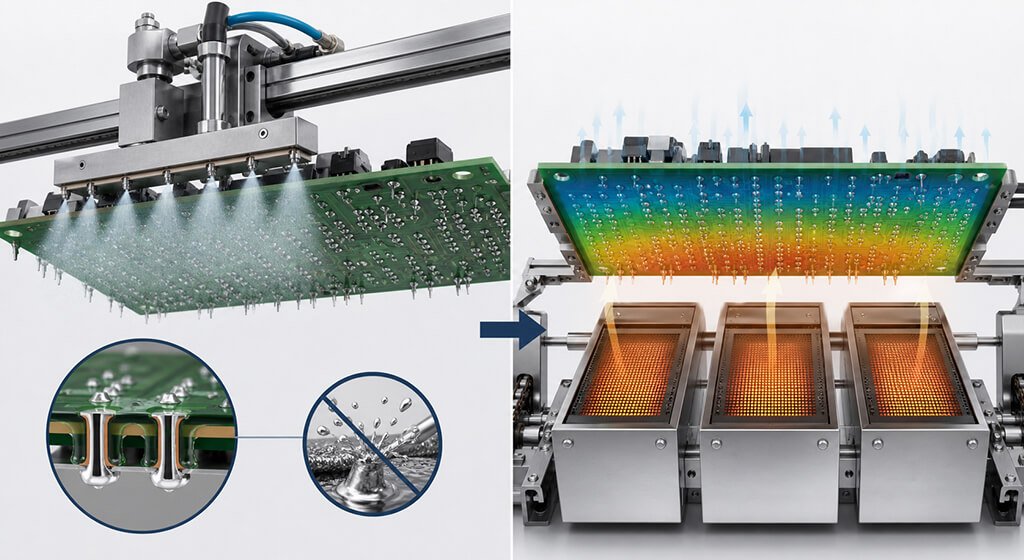
A fluxer may use a spray head, foam stone, or other delivery method. Useful controls include programmable spray areas, pressure or flow monitoring, and confirmation that the target surface received uniform coverage. Flux deposition and penetration matter more than the presence of a particular brand of fluxer.
Preheat can use infrared radiation, convection, or a combination. Top-side heating may help large component bodies and thermally massive assemblies. The available heated length determines how much energy a board can receive at a given conveyor speed.
3.2. Solder Pot, Pump, and Wave-Nozzle Geometry
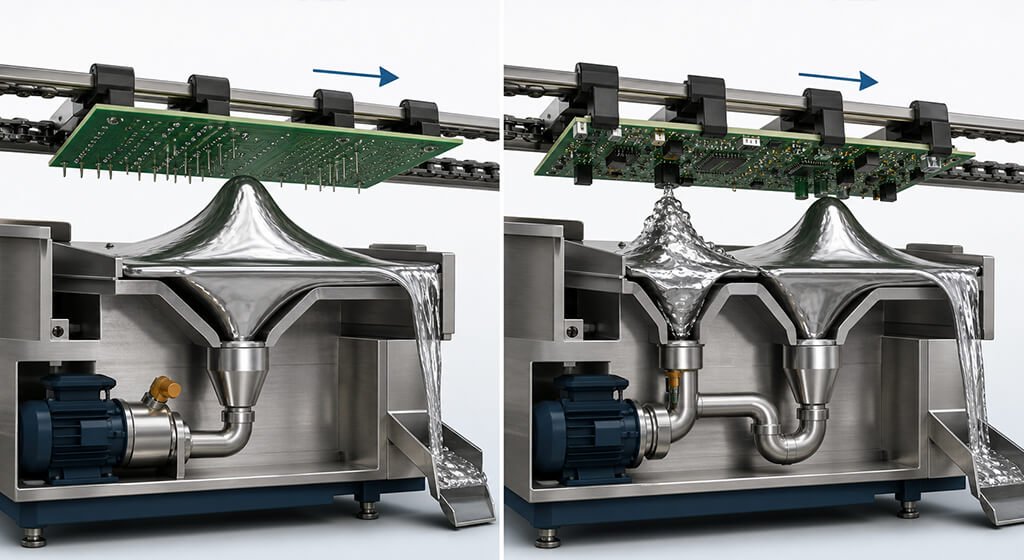
The solder module heats and circulates the alloy. It must maintain temperature, flow, and a stable contact geometry. One machine may use a single wave, a chip-plus-main arrangement, or a nozzle designed for a longer contact region.
High-thermal-mass boards may need more energy than a light single-sided board. Wider contact regions, suitable preheat, stable wave height, and board support can help. However, more contact is not always safer. Long exposure can increase component heating, copper dissolution, and material stress.
3.3. Conveyor, Board Support, and Cooling
The conveyor control speed, angle, tracking, and support. Bare boards can travel on fingers when their edges and rigidity permit it. Frames and pallets can support irregular shapes or protect bottom-side areas.
Support affects flatness and wave contact. A board that sags or lifts can experience different solder exposure across its width. The transfer into cooling and downstream inspection must also avoid shock or contact with joints that remain soft.
3.4. Nitrogen, Sensors, Alarms, and Data Logging
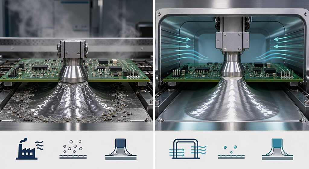
Nitrogen can reduce oxidation, improve wetting conditions, and reduce dross in a suitable system. It is not mandatory for every lead-free process. In its engineering note on nitrogen, ITW Electrovert reports that acceptable results are often possible without nitrogen. The note recommends comparing soldered output under controlled conditions.
Modern equipment may monitor oxygen, temperature, flux flow, wave height, conveyor movement, solder level, and alarms. Such features improve observability. They do not replace profiling, inspection, maintenance, or a reaction plan when a variable leaves its control limit.
4. How Is a Wave Soldering Temperature Profile Developed?
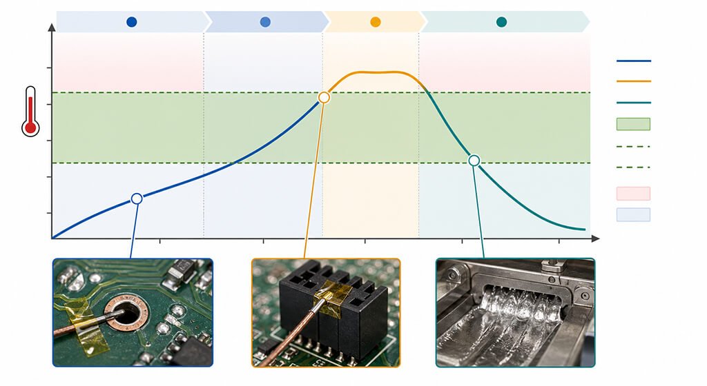
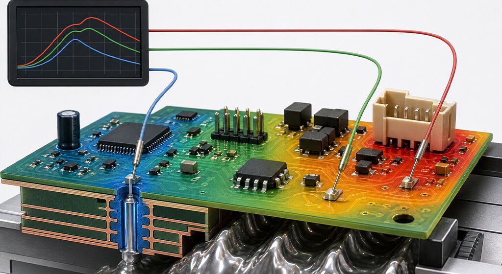
A wave soldering profile is developed by measuring the thermal response of a representative, fully populated assembly while it travels through the actual line.
Engineers place thermocouples at critical locations, compare the results with flux, alloy, PCB, and component limits, then establish a documented process window. Machine setpoints alone are insufficient evidence.
4.1. Machine Settings vs. Measured Assembly Temperatures
A pot controller reports molten solder at its sensor. A preheater controller reports a heater or zone condition. Neither value states the temperature at the top-side land, connector housing, sensitive component body, or coldest copper-connected hole.
Variable | What It Describes | Why It Cannot Stand Alone | Useful Verification |
Solder-Pot Setpoint | Controlled temperature in the solder pot | Does not show component or top-side thermal response | Calibrated pot measurement plus board profile |
Preheater Setting | Heater output or zone target | Absorption varies with board color, mass, layout, and distance | Thermocouples on representative board locations |
Conveyor Speed | Time through preheat and wave | Contact also depends on nozzle length and wave geometry | Measured travel distance and contact time |
Wave Height / Pump Setting | Solder-flow and contact condition | Board flatness, fixture design, and loading can change contact | Wave verification and solder-side observation |
Top-Side Temperature | Actual board temperature at a specific location | A single measurement point may miss the coldest or hottest region | Multiple thermocouples selected according to risk |
Component-Body Temperature | Thermal exposure experienced by a component | Temperature limits are package- and manufacturer-specific | Sensor positioned at the defined package location |
The difference matters during troubleshooting. A cold top side may limit PTH fill even while the pot remains on target. A sensitive connector body may approach its limit while a nearby low-mass joint solders correctly.
4.2. Thermocouple Placement and Measurement Traceability
Thermocouples should represent the thermal risks on the product. Likely locations include a high-copper PTH, a cold board region, a sensitive component body, a representative top-side surface, and the solder-contact area. The placement plan should state what each sensor is intended to prove.
AIM recommends using at least three thermocouples in its wave-profile supplement. The same document recommends collecting and recording profile data for each assembly part number. Those are industry recommendations from a solder-material supplier, while IPC-7530 provides the profiling framework.
Measurement quality also matters. NIST defines metrological traceability as a documented, unbroken calibration chain in which each calibration contributes to measurement uncertainty. Its traceability policy also warns that calibration alone does not prove a result is fit for purpose. The profiler, thermocouples, attachment method, sampling, and uncertainty must suit the decision.
4.3. Why Pot Temperature, Contact Time, and Conveyor Speed Interact?
The joint receives heat from preheat, molten solder, and surrounding copper. A faster conveyor may preserve throughput, but it reduces preheat exposure and solder contact unless equipment geometry changes. A slower speed can improve heat input while increasing component exposure and cycle time.
Pot temperature changes wetting kinetics and heat transfer. It can also change dross behavior, material stress, and copper dissolution. An IPC-hosted study of copper dissolution in lead-free solders found that alloy, temperature, time, and dynamic flow all affected dissolution. The results belong to the tested materials and conditions, but the interaction is directly relevant to process development.
4.4. Why There Is No Universal Lead-Free Wave Soldering Profile?
Lead-free alloys often run at higher solder-pot temperatures than traditional tin-lead alloys. That general statement does not create one correct number. The alloy’s technical data, flux window, board mass, nozzle, contact time, and component limits determine the useful range.
Component guidance illustrates this product specificity. A Melexis through-hole application note gives a 2–4 second dwell example for its stated application. It also specifies a 260°C maximum at the identified component-body location. These values are product guidance, not IPC limits for every PCBA.
5. Which Materials and Components Limit the Process Window?
The usable process window is bounded by materials that need enough heat and flux to wet, and items that can tolerate only limited exposure. Solder alloy, flux chemistry, PCB laminate, surface finish, component leads, connector plastics, adhesives, coatings, and fixtures all matter. The most restrictive verified requirement may control the complete recipe.
5.1. Lead-Free and Tin-Lead Solder Alloys
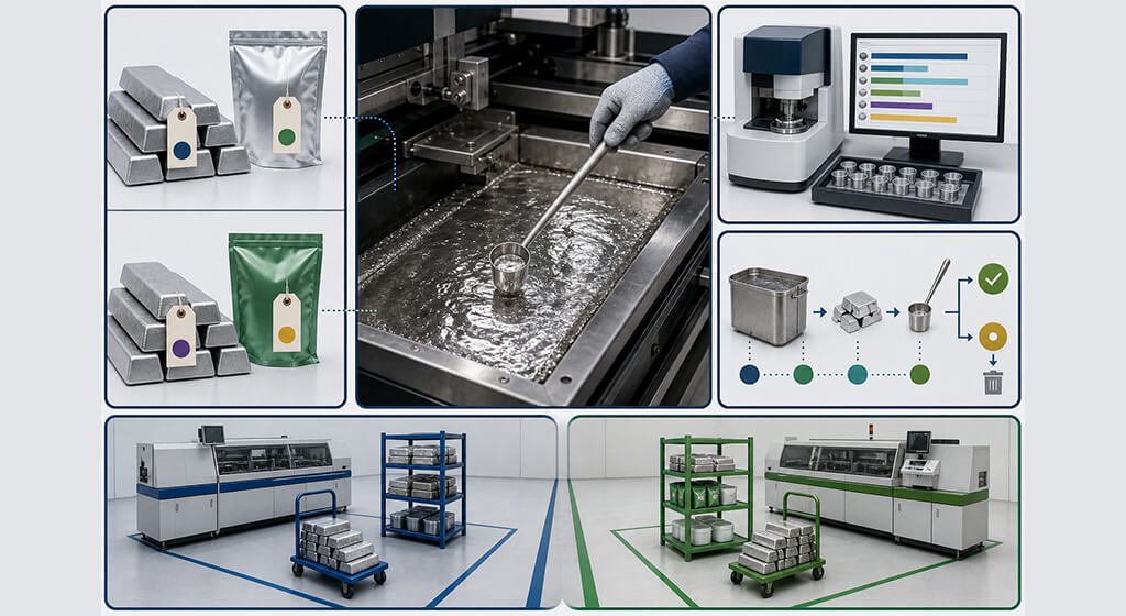
The alloy determines melting behavior and influences pot temperature, wetting, dross, cost, contamination limits, and copper dissolution. J-STD-006 defines requirements for electronic-grade solder alloys and solid solders. It does not select the optimum alloy for a particular board.
Tin-lead and lead-free production require contamination controls. A supplier should document the pot identity, replenishment material, sampling method, analysis interval, acceptance limits, and reaction plan. Separate pots, tools, or lines may be needed when customer and regulatory requirements prohibit cross-contamination.
Solder-pot analysis becomes important because copper and other metals enter the bath during production. The correct interval depends on alloy, pot size, throughput, board finishes, contact conditions, supplier recommendations, and customer requirements.
5.2. Flux Chemistry and Residue Requirements
Flux selection must consider the alloy, PCB finish, component finish, activation temperature, application system, reliability environment, cleaning plan, and downstream coating. A classification such as low- or high-activity does not describe the complete process window.
Water-based fluxes need adequate drying before molten solder contact. Incomplete drying can cause spattering and solder balls. Water-soluble flux residues usually require thorough cleaning according to the supplier’s current data. No-clean residues still need validation when high voltage, low standoff, humidity, conformal coating, or high-reliability service raises electrochemical risk.
5.3. Component Solderability and Thermal Limits
Lead finish, age, storage, contamination, and handling affect component solderability. A thermally adequate profile cannot compensate for a badly oxidized termination indefinitely. J-STD-002 provides component solderability test methods when such testing is invoked.
Component bodies may face heat conducted along metal leads. This is especially important for connectors with plastic housings, sensors, optoelectronics, switches, and parts close to the board. The applicable manufacturer data sheet or package document must control.
Full-body immersion of an SMD is a separate risk from lead-only exposure of a THT part. Vishay’s current soldering-process guidance warns against generalizing full-body wave exposure to its SMD packages and calls for user evaluation where applicable.
5.4. PCB Material, Surface Finish, and Storage
The PCB must survive the cumulative thermal history of fabrication, reflow, wave soldering, and rework.
Tg, decomposition temperature, z-axis expansion, time-to-delamination data, moisture, plated-hole construction, and actual cycle count provide different information. Tg alone is not a maximum soldering temperature.
Surface finish and storage also affect wetting. J-STD-003 provides solderability tests for printed boards. If a finish has exceeded its supported storage period or shows contamination, the team should assess the board rather than compensating blindly with more heat or flux.
6. How Should a PCB Be Designed for Wave Soldering?
A wave-solderable PCB gives flux, heat, and molten solder reliable access to every intended joint while protecting incompatible features.
Designers must coordinate hole and lead tolerances, copper connections, component orientation, bottom-side clearances, lead protrusion, board support, and pallet openings.
Early design for manufacturability (DFM) reduces reliance on narrow process settings and rework.
Design Feature | Manufacturing Mechanism | Risk if Poorly Controlled | Information Needed for DFM |
Finished Hole and Lead | Controls insertion clearance and capillary path | Difficult insertion, weak solder flow, inconsistent fill | Lead maximum/minimum, finished-hole tolerance, plating, customer acceptance criteria |
Copper-Plane Connection | Draws heat away from the joint | Cold top side and insufficient solder fill | Layer stack-up, copper weights, plane count, thermal-relief intent |
Component Orientation | Affects shadowing and solder drainage | Skips, bridging, and excess solder | Conveyor direction, component body and lead geometry |
Lead Protrusion | Influences solder contact and drainage | Flags, bridges, and poor fillet visibility | Controlled trim range and component seating requirements |
Bottom-Side SMD Clearance | Determines wave access and thermal exposure | Package damage, shadowing, or unintended solder contact | Package approval, adhesive type, keep-outs, wave type |
Pallet Opening and Wall | Controls flux, heat, and solder access | Low fill, poor drainage, and trapped residue | Opening dimensions, wall thickness, material, support, wear limits |
6.1. Finished-Hole Size, Lead Clearance, Lands, and Annular Rings
The finished hole must accept the lead across worst-case tolerances and still support solder flow. Designers should use the actual component drawing, not a nominal lead dimension copied from a library. Hole plating and fabrication tolerances reduce the available opening.
Excessive clearance can reduce capillary behavior or create a solder-volume problem. Insufficient clearance can prevent insertion and restrict flux or solder movement. There is no one lead-to-hole ratio that fits round leads, square connector pins, irregular terminals, press-fit alternatives, and every product class.
Land and annular-ring design must meet the applicable board specification and assembly needs. Solder-mask registration, nearby copper, and escape routing should be reviewed together.
6.2. Board Thickness, Copper Planes, and Thermal Relief
Thicker boards create a longer barrel and often carry more copper. Plane-connected holes can remove heat faster than isolated holes. A profile that solders a signal pin may leave a nearby ground pin with low top-side fill.
An IPC-hosted hole-fill study showed that board thickness, connected ground planes, copper thickness, and component type affected fill. Its test vehicles are not universal limits. The practical lesson is to identify high-mass joints during DFM and place thermocouples accordingly.
Thermal relief can reduce the heat drawn into a plane, but electrical, current, mechanical, and reliability requirements may restrict its use. The PCB designer and assembler should agree on the tradeoff before release.
6.3. Component Orientation, Spacing, Shadowing, and Lead Protrusion
Board travel direction changes how solder reaches and leaves a component. Closely spaced rows, large bodies, and downstream pads can create shadowing. Orientation also affects whether excess solder drains away or remains between neighboring leads.
Lead protrusion should support contact and inspection without creating unnecessary bridging risk. The correct range depends on component seating, joint geometry, board thickness, fixture, and invoked acceptance criteria. A documented trim requirement is better than an arbitrary universal value.
6.4. Bottom-Side SMD Components, Adhesive, and Wave Clearance
Only qualified packages and suitable land patterns should face full-body wave exposure. Adhesive must hold the device through fluxing, preheat, solder contact, and cleaning. Its cure process also becomes part of the assembly’s thermal history.
Large bodies can shadow downstream pads. Fine-pitch parts may bridge if orientation and drainage are poor. Components with moisture, seal, optical, plastic, or stress sensitivity need special attention. Manufacturer data takes priority over a generic “wave solderable” label in a component library.
6.5. Pallet Openings, Masking, and Board Support
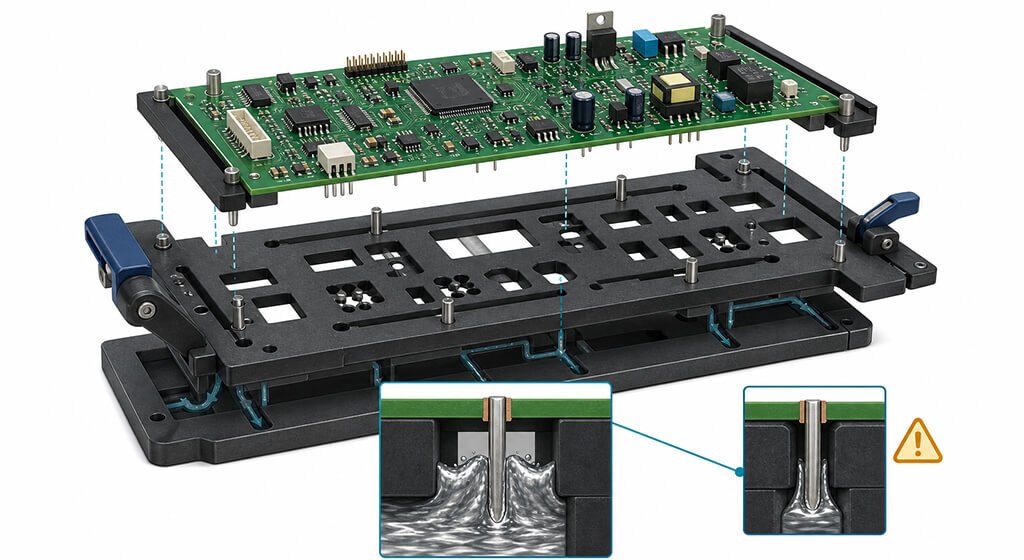
A selective pallet can expose only intended areas while shielding bottom-side components. It can make a mixed board practical, but it does not remove all design limits. Pallet walls can block spray flux, reduce preheat, restrict wave reach, and change drainage near an opening.
The pallet material, thickness, moisture condition, support points, and accumulated contamination affect repeatability. Its drawing and revision should be controlled. Worn or damaged pallets need defined rejection criteria.
7. What Are the Most Common Wave Soldering Defects?
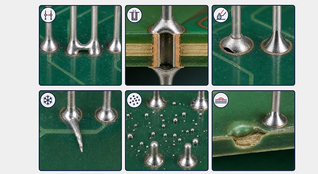
Common defects include bridging, insufficient PTH fill, nonwetting, dewetting, solder skips, icicles, flags, solder balls, pinholes, and heat damage.
Each symptom has several possible causes. Effective troubleshooting starts by mapping the defect pattern, collecting process and material evidence, then changing controlled variables while verifying the result.
7.1. Start with the Defect Pattern Before Changing the Recipe
First determine whether the defect repeats on the same joint, component, board region, panel position, or production interval. A fixed ground pin suggests a different investigation from random solder balls across the assembly. A defect appearing after a material change or maintenance event also narrows the search.
Review the profile, recipe revision, flux and alloy lots, component and PCB lots, pot analysis, pallet identity, alarm history, inspection images, and rework data. Change one factor at a time where practical. A simultaneous increase in flux, heat, and contact time may hide the actual cause and create a new risk.
Defect | Likely Causes | Detection and First Checks | Prevention and Controlled Action |
Bridging | Poor drainage, unfavorable orientation, excessive lead protrusion, unstable exit, weak solderability | Map defect locations; inspect solder side; check lead dimensions, orientation, conveyor stability, and wave-contact records | Design for drainage; control lead protrusion and orientation; adjust one validated exit or contact variable at a time |
Insufficient Top-Side Fill | High thermal mass, weak flux penetration, poor solderability, restrictive hole geometry, limited contact | Profile the cold joint; review stack-up, plane connections, flux coverage, surface finish, and lead condition | Address the demonstrated heat, access, geometry, or surface issue without exceeding component limits |
Nonwetting or Solder Skips | Oxidation, contamination, inadequate flux or activation, insufficient heat, surface finish or solder-mask issue | Check incoming lots, surface condition, flux coverage, storage history, and thermal profile | Protect solderability; control storage and handling; validate flux application and preheat |
Icicles or Flags | Poor drainage, excessive lead length, unfavorable orientation, separation conditions | Measure lead protrusion; review orientation, exit images, conveyor angle, and recipe | Specify lead trim and drainage-friendly orientation; control separation conditions |
Solder Balls or Spatter | Moisture, trapped solvent, outgassing, turbulence, pallet or mask condition | Review preheat, flux condition, board moisture exposure, pallet history, and defect distribution | Keep boards and pallets dry; verify flux drying; correct excessive turbulence |
Board, Laminate, or Component Damage | Excessive heat, moisture, repeated thermal exposure, violated material or component limits | Reconstruct full thermal history; verify laminate grade, moisture controls, and component limits | Use qualified materials; control cumulative passes and rework; profile sensitive locations |
7.2. Solder Bridging
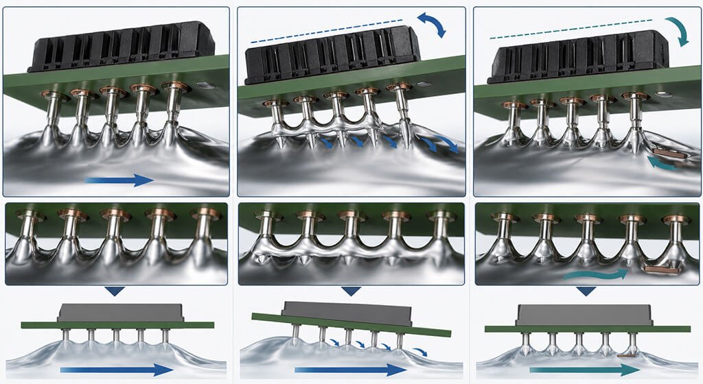
A bridge forms when solder creates an unintended electrical connection. It often appears between adjacent leads or lands, but the underlying cause may sit elsewhere. Poor drainage, excessive protrusion, unfavorable orientation, wave instability, conveyor vibration, contamination, and weak solderability can all contribute.
Start with geometry and repeatability. If the same last pins on a connector bridge, examine travel direction, lead length, pad arrangement, and wave separation. If bridges move randomly, review flux uniformity, wave stability, pot condition, conveyor motion, and material variation.
Reducing wave height or contact time may help one case and create insufficient fill elsewhere. The correction should preserve the validated thermal and wetting needs of the coldest joints.
7.3. Insufficient Top-Side Hole Fill
Insufficient fill means solder has not risen through the barrel to the required level or wetted the intended surfaces. Possible causes include inadequate joint heat, weak flux penetration or activation, and poor PCB or lead solderability. Hole-to-lead geometry, pallet obstruction, or insufficient wave contact may also restrict fill.
Use a thermocouple at the problem location when heat is suspected. A profile measured only on an easy signal pin does not represent a ground pin tied to several planes. Review the PCB stackup and copper connections before increasing pot temperature.
Do not use 100% fill as an automatic universal requirement. Acceptance depends on the exact joint, product class, customer drawing, and current licensed criteria. Engineering reliability studies can explain mechanisms, but they do not replace the invoked acceptance standard.
7.4. Nonwetting, Dewetting, and Solder Skips
Nonwetting occurs when solder fails to form the required bond to a surface. Dewetting describes solder that initially wets and then recedes, leaving an irregular condition. A skip is an area or joint that receives little or no solder. These observations should not be treated as synonyms during root-cause analysis.
Inspect PCB lands, component leads, storage, oxidation, contamination, surface finish, mask condition, flux coverage, and temperature. Increasing flux activity may disguise a material problem without making the supply chain reliable. Solderability testing under J-STD-002 or J-STD-003 may be appropriate when incoming surfaces are in doubt.
7.5. Icicles, Flags, and Excess Solder
An icicle or flag is a protruding solder formation that remains after separation. Long or contaminated leads, unfavorable drainage, excessive solder retention, weak wetting balance, low exit temperature, or unstable separation can contribute.
Measure lead protrusion and check where the formation points relative to travel. Compare the defect across identical components and panel positions. A mechanical drawing or trim correction may produce a more robust result than repeatedly changing the global recipe.
7.6. Solder Balls, Spattering, Pinholes, and Voids
Solder balls and spatter can result when moisture or volatile material reaches molten solder. Inadequate flux drying, wet pallets, absorbed board moisture, mask behavior, or excessive turbulence are possible domains. A hot pot does not prove that the solvents were removed before contact.
Pinholes and visible void-like openings can involve outgassing, surface condition, barrel geometry, flux behavior, or solidification. The visible symptom alone cannot locate an internal void. Select an inspection method that matches the risk and acceptance requirement.
7.7. Board Damage, Delamination, or Component Damage
Thermal damage can appear as discoloration, warpage, delamination, lifted features, cracked packages, or deformed connector bodies. Review the cumulative process, including prior reflow, wave passes, touch-up, and rework. The final damaging event may not be the only exposure that mattered.
Material selection and storage are part of the investigation. So are thermocouple locations. A sensor far from a sensitive plastic housing cannot demonstrate that the housing stayed within its limit.
8. How Are Wave-Soldered Assemblies Inspected and Accepted?
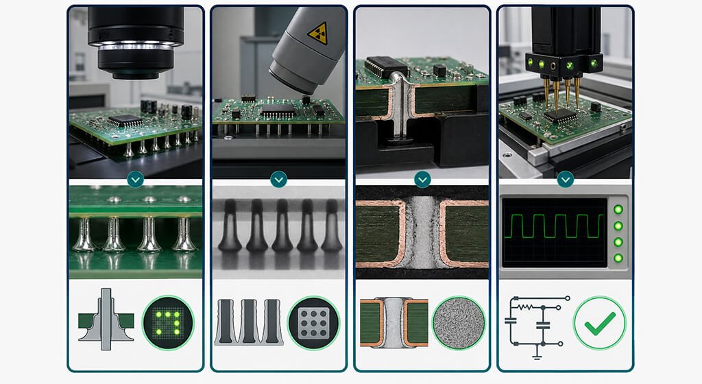
PCB Inspection combines visible workmanship review, targeted internal analysis, and electrical or functional testing. Acceptance must follow the customer-invoked requirements and product class. J-STD-001 addresses soldered-assembly materials and process requirements, while IPC-A-610 addresses post-assembly acceptability. Inspection equipment does not replace the applicable criteria or process records.
8.1. Visual Inspection and AOI
Visual inspection can identify bridges, missing solder, poor visible fillets, flags, residue, damage, orientation errors, and lead conditions. Automated optical inspection (AOI) can improve repeatability and coverage when camera access, lighting, programming, and review rules suit the joint.
AOI cannot see every internal barrel condition. Tall components and connectors can block the view.
8.2. X-Ray, Microsection, and Destructive Analysis
X-ray may help with hidden solder distribution or internal anomalies when geometry and equipment permit useful interpretation. It is not the default answer for every visible THT joint. Image quality, angle, overlap, and operator interpretation affect what can be concluded.
Microsection provides a direct internal view at the cut location. It can support process qualification, failure analysis, or investigation of fill, plating, and damage. Because it is destructive and samples limited locations, the sectioning plan must represent the question being investigated.
8.3. Electrical and Functional Testing
Open-short testing, in-circuit testing (ICT), boundary scan, or functional circuit testing (FCT) can detect electrical failures that visual inspection misses. The choice depends on test access, volume, fixture cost, firmware, product risk, and customer requirements.
An assembly can pass a functional test while containing a workmanship condition that violates its procurement specification. It can also look acceptable but fail electrically. Product acceptance may therefore require both workmanship inspection and electrical evidence.
8.4. J-STD-001, IPC-A-610, and Product Classes
IPC describes J-STD-001J as the industry-consensus requirements standard for soldered electrical and electronic assemblies. IPC-A-610J is its post-assembly acceptability counterpart. The IPC announcement for the J revisions explains their complementary roles.
Class 1, 2, or 3 should be invoked by the customer or procurement documents. A statement that an inspector is trained to IPC-A-610 does not make every product Class 3. The drawing, contract, materials, process controls, inspection, objective evidence, and acceptance must support the required class.
8.5. Process Records That Support Repeatability
A release record should identify the assembly and recipe revisions, material lots, profile status, first-article result, inspection, test, deviations, and rework. Supporting process records may include flux verification, solder-pot analysis, alarm history, pallet identity, and calibrated equipment status.
These records help distinguish a stable process from a shipment that merely passed final sampling. They also shorten root-cause analysis when a field, customer, or later-production issue appears.
9. Is Wave Soldering Still Used in Modern PCB Assembly?
Yes. Wave soldering remains useful for stable assemblies with many accessible THT joints and for selected mixed-technology products.
Its role is narrower than when leaded components dominated PCB design, but modern power electronics, industrial controls, appliances, communications equipment, and connector-rich products still create suitable applications.
Process choice must follow the board, not its age or industry label.
Use the following table as an early process-screening tool. Final selection still requires design-for-manufacturing (DFM) review, component limits, acceptance criteria, volume, and total-cost analysis.
Project Condition | Strong Starting Candidate | Why It May Fit | Validate Before Release |
Many accessible THT joints on a stable, repeating assembly | Wave Soldering | One conveyor pass can form many joints efficiently | Bottom-side access, pallet openings, drainage, component limits, thermal profile, and acceptance evidence |
Mostly SMT, with paste-compatible THT pins | Reflow or Pin-in-Paste | May eliminate a separate soldering operation | Paste volume, stencil design, connector coplanarity, component reflow rating, and void or fill criteria |
A few scattered THT joints on a dense mixed-technology board | Selective Soldering | Local flux and mini-wave contact can protect nearby features | Nozzle access, keep-outs, cycle time, solderability, and localized thermal profile |
One unusual or heat-sensitive component, or a very small prototype run | Controlled Robotic or Manual Soldering | Local handling may avoid a complex pallet and full-line setup | Operator or program qualification, tip access, thermal exposure, inspection, and repeatability |
A connector designed and qualified for compliant press-fit termination | Press-Fit | Avoids a solder thermal cycle at those pins | Hole and pin tolerances, insertion force, tooling, board support, and qualification requirements |
Different joint groups have conflicting access or thermal needs | Hybrid Route | Each method can be applied to the joint group it controls best | Process sequence, cumulative thermal history, masking, cleanliness, inspection, and rework limits |
9.1. Where Wave Soldering Still Has a Strong Fit
Wave soldering can be efficient when many joints form during one pass. Stable product geometry allows the manufacturer to reuse a validated recipe and controlled pallet. The method also offers strong solder contact across a broad area when the underside is designed for it.
The best candidates often have repeated THT patterns, accessible lands, tolerant components, and predictable production demand.
High volume helps, but annual quantity alone is not decisive. Batch size, product mix, setup time, line loading, inspection, and change frequency also matter.
9.2. Where Wave Soldering Is Poorly Fit?
The process becomes less attractive when only a few THT joints remain or sensitive bottom-side parts occupy the solder side. Dense mixed technology may require complex pallets with narrow openings. Those openings can restrict flux, heat, solder contact, and drainage.
Very high product mix can also reduce the value of a full-width process. Frequent pallet and recipe changes consume engineering and production time. Localized selective, robotic, or manual methods may be more practical after total-cost and risk review.
9.3. Why Modern Production Often Uses a Hybrid Process
A single PCBA may use reflow for SMDs, wave for an accessible THT group, selective soldering for protected joints, and controlled hand soldering for a special component. Press-fit or pin-in-paste may remove other joints from the wave step.
This is normal process planning, not a compromise by default. Each method should solve the geometry, thermal, volume, quality, and commercial requirements of its assigned joints.
10. Wave Soldering vs. Reflow and Selective Soldering
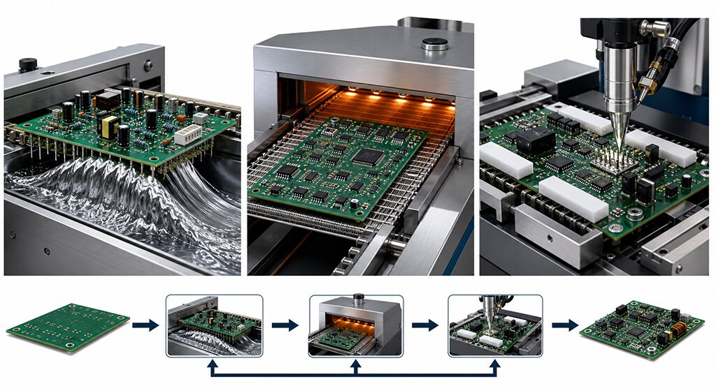
Wave, reflow, and selective soldering apply heat and solder differently. Reflow normally melts deposited solder paste across an SMT assembly. Wave soldering contacts a broad bottom-side area with flowing molten solder. Selective soldering applies flux and a mini-wave to defined THT locations. Mixed assemblies may use two or all three processes.
Factor | Wave Soldering | Reflow Soldering | Selective Soldering |
Typical Joint Set | Many accessible THT joints; approved bottom-side SMDs | SMT joints and suitable pin-in-paste THT | Selected THT joints on mixed-technology boards |
Solder Delivery | Molten solder wave contacts an exposed area | Printed or dispensed solder paste is heated through a reflow profile | Local mini-wave, drag, dip, or multi-nozzle tool |
Thermal Exposure | Primarily solder side plus conducted and preheat energy | Most of the assembly passes through the oven thermal profile | Local solder contact plus product preheating |
Main Advantage | Forms many joints efficiently in one conveyor pass | Supports dense, highly automated SMT assembly | Provides localized access and programmable joint treatment |
Main Design Constraint | Bottom-side access, drainage, pallet design, and thermal balance | Paste printing, component placement, and package/reflow limits | Nozzle access, keep-outs, cycle time, programming, and tooling |
10.1. Wave Soldering vs. Reflow Soldering
Reflow normally starts with solder paste printed on surface lands. Components are placed, and the full assembly passes through a thermal profile that melts the paste. Wave soldering starts with liquid flux and uses a molten solder wave to supply solder and heat from the bottom.
The distinction is not simply “wave for THT and reflow for SMT.” Pin-in-paste can reflow compatible through-hole parts. Approved bottom-side SMDs can face a wave. Component geometry, solder volume, package limits, equipment, and production economics determine the route.
10.2. Wave Soldering vs. Selective Soldering
Wave soldering exposes an accessible bottom-side region and can form many joints in one pass. Selective soldering targets defined joints with a local nozzle or tool. Wave often suits stable THT-heavy products, while selective often suits mixed boards, restricted undersides, scattered THT joints, or high product mix.
Neither method is automatically cheaper or higher quality. Pallet cost, program time, nozzle access, throughput, flux and nitrogen use, inspection, rework, and changeover determine total cost. Compare the complete production route and defect risk rather than equipment cycle time alone.
10.3. Other THT Attachment Options
Pin-in-paste uses solder paste and reflow for compatible THT joints. Press-fit creates a mechanical and electrical connection without solder. Robotic or manual soldering can handle unusual parts or small quantities. Each option introduces its own component, hole, tooling, inspection, and reliability requirements.
11. FAQ About Wave Soldering
What is the purpose of wave soldering?
Wave soldering forms many accessible solder joints during one controlled conveyor pass. It is mainly used for through-hole assemblies and compatible mixed-technology boards. Its value comes from repeatable mass soldering, not simply high heat. The process still requires suitable PCB design, solderable materials, controlled flux and alloy, product-specific profiling, and inspection.
What temperature is used for lead-free wave soldering?
There is no universal lead-free pot temperature. The acceptable range depends on the solder alloy, flux, wave geometry, contact time, board thermal mass, and component limits. Supplier data may offer starting ranges, but engineers must measure the actual assembly. A pot setpoint cannot prove top-side PTH fill or component-body compliance.
How long should a PCB contact the solder wave?
Required contact time depends on wave length and geometry, conveyor speed, alloy, flux, board mass, pallet, and joint design. Component documents may also set maximum exposure. Published examples such as 2–4 seconds belong to a defined supplier or component context. The approved value must satisfy wetting and fill without exceeding material limits.
Why is preheating required before wave soldering?
Preheating removes volatile flux carriers, activates the flux, reduces thermal gradients, and supplies energy to the PCB and components. It is especially important for thick boards, copper planes, and pallets. Too little preheat can cause weak wetting or spattering. Too much can consume flux activity or overheat materials and components.
What causes insufficient through-hole solder fill?
Start with heat, flux, and solderability. Plane-connected copper, restrictive hole-to-lead geometry, short contact, low wave access, or pallet obstruction can also limit fill. Profile the actual cold joint and review the stackup before changing the recipe. A higher pot temperature is not automatically the correct fix.
12. Final Takeaway: Validate the Assembly, Not a Generic Recipe
Reliable wave soldering comes from matching the process to the PCB, components, materials, equipment, and acceptance requirements. Use published ranges as evidence and starting guidance, not universal rules. Measure the populated assembly, protect its most restrictive limits, inspect the resulting joints, and retain records that show the approved process remained under control.
Wave soldering is a strong fit when the design provides broad solder access. A product-specific profile must also achieve reliable wetting without exceeding material or component limits. When those conditions cannot be demonstrated, selective soldering, reflow, press-fit, robotic soldering, or a hybrid route may be safer.
Early DFM is often the most economical control. Send the supplier complete fabrication data, BOM, assembly drawings, quantities, and acceptance requirements before the design is frozen. That information allows the team to select wave soldering where it fits and propose a different route where it does not.