
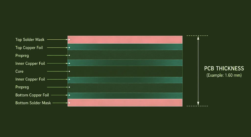
PCB thickness is the finished distance between a manufactured board’s two outer surfaces, including applied coatings.
For standard rigid FR-4, 1.57 mm or 1.60 mm usually provides the practical starting point.
The correct value still follows connector fit, enclosure space, mechanical loading, stackup geometry, and fabrication capability.
Finished PCB thickness differs from individual copper, dielectric, solder-mask, and surface-finish measurements listed inside your stackup.
Searchers sometimes call the same measurement **PCB board thickness**, although engineers usually prefer finished PCB thickness.
Table of Contents
1. What Is the Standard PCB Thickness?
The familiar value began with historical 1/16-inch insulating sheets, measuring exactly 1.5875 mm under NIST conversion.
Modern suppliers may describe nearby nominal options as 1.57 mm, 1.60 mm, 0.062 inch, or approximately 62 mil.
These conventions explain current availability, but no single IPC reference makes 1.60 mm compulsory for every rigid board.
Treat both values as widely supported starting points, then confirm your complete product requirements before release.
1.1. Why Do You Often See 1.57 mm?
Record the defect location, production lot, panel position, component reference, and inspection stage. Photograph everything before cleaning, heating, bending, scraping, or removing any component from the assembly.
Compare affected boards against known-good boards from the same lot and another production lot. Save available SPI, AOI, X-ray, reflow, placement, electrical, and functional test records.
Determine whether the defect appeared after reflow, depaneling, connector insertion, housing installation, or reliability testing. That timing often narrows your investigation faster than visual inspection alone and avoids unnecessary destructive checks.
1.2. Are 1.50 mm, 1.57 mm, and 1.60 mm Identical?
Treat 1.50 mm, 1.57 mm, and 1.60 mm as separate nominal specifications during design and procurement.
Overlapping manufacturing tolerances never make those nominal values interchangeable across connectors, rails, or press-fit components.
State both nominal finished thickness and permitted tolerance wherever mechanical fit controls product performance or assembly.
1.3. How Do You Convert PCB Thickness Between Millimeters, Inches, and Mils?
NIST unit definitions establish 25.4 millimeters per inch and 0.0254 millimeter per mil for reliable conversion.
Nominal PCB Thickness | Inches | Mils |
0.20 mm | 0.00787 in | 7.87 mil |
0.40 mm | 0.01575 in | 15.75 mil |
0.60 mm | 0.02362 in | 23.62 mil |
0.80 mm | 0.03150 in | 31.50 mil |
1.00 mm | 0.03937 in | 39.37 mil |
1.20 mm | 0.04724 in | 47.24 mil |
1.50 mm | 0.05906 in | 59.06 mil |
1.57 mm | 0.06181 in | 61.81 mil |
1.5875 mm | 0.06250 in | 62.50 mil |
1.60 mm | 0.06299 in | 62.99 mil |
2.00 mm | 0.07874 in | 78.74 mil |
2.40 mm | 0.09449 in | 94.49 mil |
3.20 mm | 0.12598 in | 125.98 mil |
These exact conversions explain why 1.57 mm and 1.60 mm remain similar, although they are not identical.
2. Which Common PCB Thickness Should You Choose?
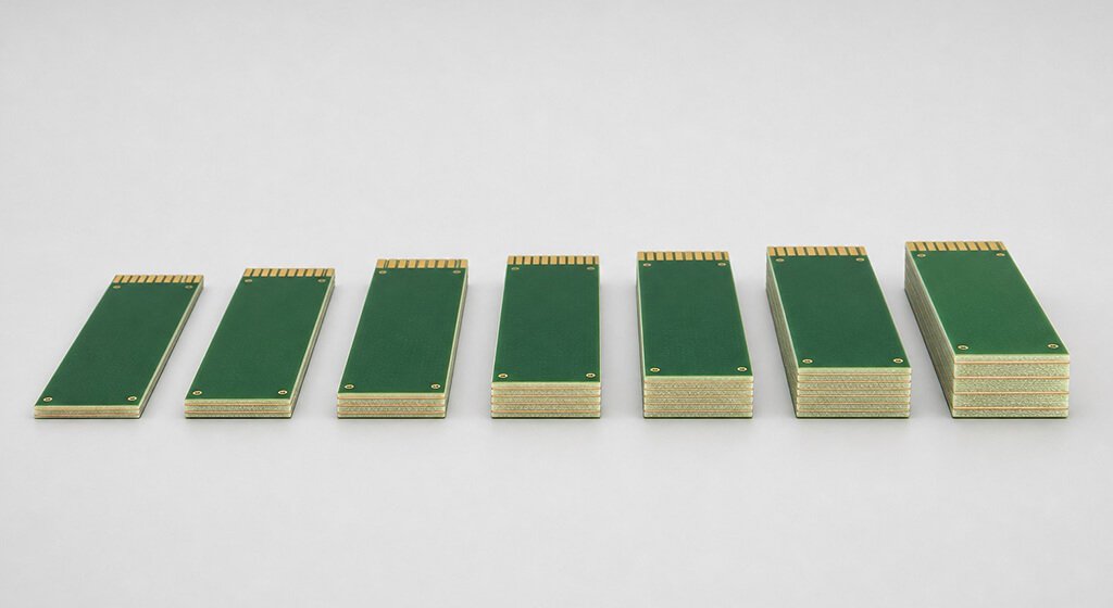
Common rigid PCB thickness options range from ultra-thin 0.20 mm constructions through heavy 3.20 mm boards.
Use this **PCB thickness chart** during planning, then confirm material availability before finalizing your production stackup.
PCB Thickness | Typical Applications | Main Benefit | Main Concern |
0.20–0.40 mm | Sensors, compact modules, miniature products | Save space and weight | You face handling, warpage, finish, and assembly limits |
0.60 mm | Wearables, portable modules, compact controls | Gain a thin construction | You receive less rigidity than thicker boards |
0.80 mm | Keyboards, compact electronics, small modules | Balance space and availability | Your main checks are connectors and enclosure support |
1.00 mm | Consumer products, communication modules | Reduce profile while keeping useful strength | Your stackup and panel handling need confirmation |
1.20 mm | Compact multilayer products, keyboards | Gain moderate rigidity | Your supplier must confirm material availability |
1.57–1.60 mm | General rigid FR-4 electronics | Receive broad material and connector support | Your compact product may not need this thickness |
2.00 mm | Industrial controls, larger boards | Gain improved rigidity | You increase weight and drilling difficulty |
2.40–3.20 mm | Backplanes, heavy assemblies, special connectors | Support greater mechanical loads | Your holes, connectors, and fabrication limits need review |
Ask whether your fabricator stocks the preferred construction, since mature stackups usually reduce pricing and lead times.
Choose a custom size only when your enclosure, connector, mechanics, or signal requirements provide measurable benefits.
3. How Should You Choose the Right PCB Thickness?
Choose PCB thickness through seven connected checks covering mechanical fit, electrical behavior, and realistic fabrication limits.
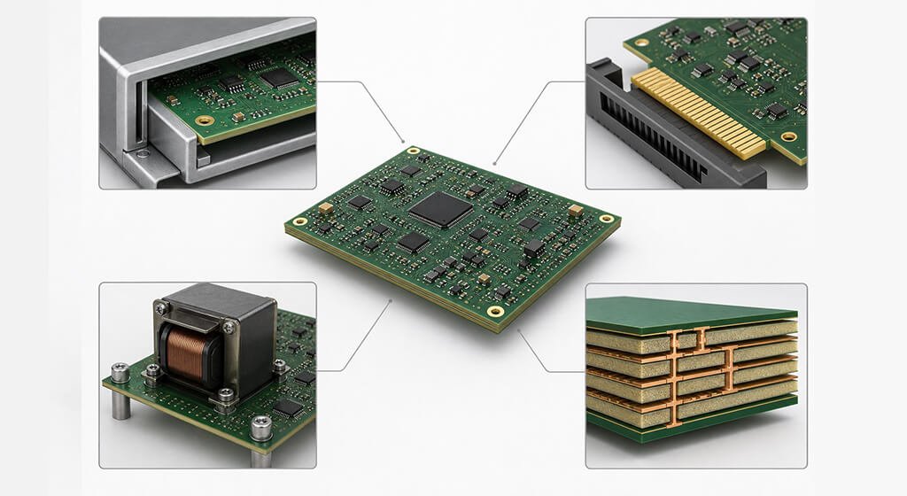
Step 1. What Does Your Enclosure Require?
Choose PCB thickness through seven connected checks covering mechanical fit, electrical behavior, and realistic fabrication limits.
Step 2. Which Connectors Will You Use?
Review every connector and press-fit component because manufacturer drawings may demand tight nominal thickness and tolerance limits.
Step 3. How Many Layers Do You Need?
Count required signal, power, ground, and shielding layers before building a manufacturable dielectric and copper stack.
Step 4. What Mechanical Loads Will You Apply?
Evaluate board area, component weight, vibration, insertion force, and unsupported spans before adding thickness or supports.
Step 5. Which Electrical Targets Must You Meet?
Define impedance, isolation, current, and thermal targets because reliable calculations require accurate copper and dielectric data.
Step 6. Can Your Fabricator Build the Stack Reliably?
Choose PCB thickness through seven connected checks covering mechanical fit, electrical behavior, and realistic fabrication limits.
Step 7. Have You Approved the Final Stackup?
Approve the final stackup before routing impedance-controlled traces, then retain its revision inside manufacturing documentation.
Design Requirement | Likely Direction | Main Check |
Ultra-thin product | Choose a thinner board | Check handling, warpage, assembly, and panelization |
Heavy components | Increase thickness or add support | Check spans, mounting points, vibration, and weight |
Edge connector | Follow its connector drawing | Check nominal thickness and tolerance |
High layer count | Develop a complete stackup | Check dielectrics, vias, and lamination cycles |
High current | Prioritize copper geometry | Check temperature rise and cooling paths |
Controlled impedance | Start from the stackup | Check Dk, dielectrics, copper, and trace geometry |
4. What Does Finished PCB Thickness Include?
Finished PCB thickness combines pressed, plated, and coated materials, so raw laminate values cannot predict final measurements.
Fabricators must account for resin flow, copper distribution, lamination pressure, plating buildup, coatings, and material tolerances.
Construction Element | What You Should Understand |
Core | A cured dielectric sheet often carries copper on both surfaces |
Prepreg | Resin-coated glass layers bond cores and copper during lamination |
Copper Foil | Copper foil creates traces, pads, planes, and conductive paths |
Plated Copper | Electroplating adds copper inside holes and across outer surfaces |
Solder Mask | Solder mask protects circuitry and covers exposed outer copper |
Surface Finish | ENIG, HASL, OSP, tin, or silver protects exposed pads |
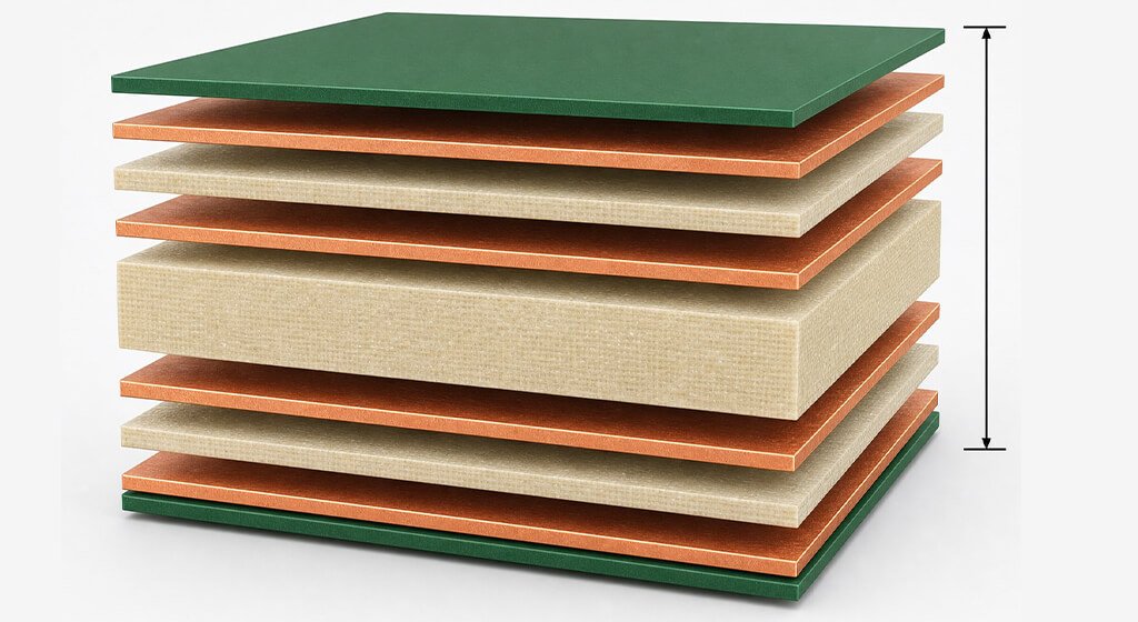
4.1. How Does Your Core Affect Board Thickness?
A cured core provides the stable dielectric foundation supporting electrical spacing, material selection, and mechanical strength.
Before calculating any stackup, confirm whether your supplier’s stated core thickness already includes attached copper cladding.
Isola’s 370HR data sheet provides one example, listing laminate thicknesses from 0.05 mm through 3.2 mm.
Those product-specific values illustrate available constructions, but never define universal limits across every FR-4 material family.
4.2. How Does Prepreg Change Your Finished Thickness?
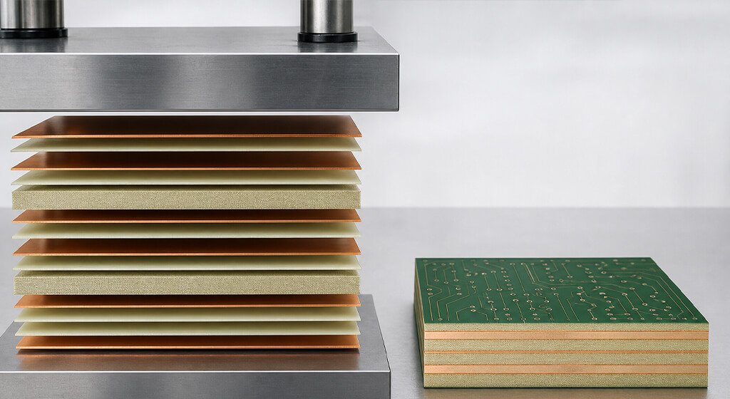
During lamination, prepreg resin flows between copper features while bonding cores and conductive layers into one board.
Catalog thickness cannot predict pressed results accurately, so request a production stackup whenever dimensional control matters.
4.3. Does Copper Thickness Equal PCB Thickness?
Total board thickness differs from copper callouts expressed through ounces per square foot, micrometers, or foil designations.
IPC-4562B supplies formal foil terminology, while these rounded conversions support practical discussions during early supplier reviews.
Copper Weight | Nominal Copper Thickness | Approximate Thickness |
0.5 oz/ft² | 17.5–18 µm | 0.69 mil |
1 oz/ft² | About 35 µm | 1.38 mil |
2 oz/ft² | About 70 µm | 2.76 mil |
3 oz/ft² | About 105 µm | 4.13 mil |
4 oz/ft² | About 140 µm | 5.51 mil |
Treat every number as nominal because electroplating usually makes finished outer copper thicker than its starting foil.
Review heavy copper PCB manufacturing when substantial current demands greater conductor thickness, wider traces, or stronger thermal planning.
5. How Thick Is a PCB at Different Layer Counts?
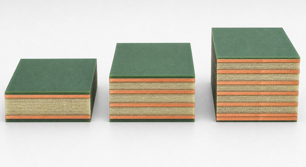
Layer count alone cannot determine finished PCB thickness because identical counts can use very different dielectric constructions.
Build every stackup around mechanical, electrical, and fabrication requirements instead of copying another board’s dimensions.
Layer Count | Common Planning Range | What You Should Confirm |
1–2 layers | 0.6–1.6 mm | Check rigidity, panel support, connectors, and surface finish |
4 layers | 0.8–2.0 mm | Check plane spacing, impedance, copper, and available prepreg |
6–8 layers | 1.0–2.4 mm | Check dielectrics, drilling, registration, and lamination |
10 or more layers | 1.2–3.2 mm or custom | Confirm via ratios, sequential lamination, and material availability |
Use these ranges only during concept planning because your approved stackup may legitimately fall outside them.
5.1. How Thick Is a Two-Layer PCB?
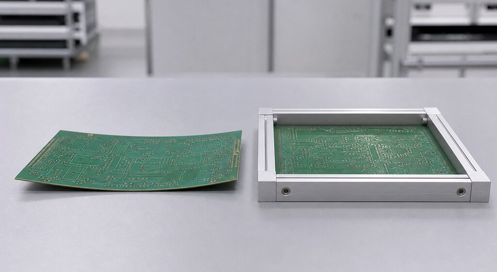
A typical 2 layer PCB thickness may be 0.6, 0.8, 1.0, 1.2, or 1.6 mm.
Thin constructions reduce weight and profile, while thicker boards better support heavy components or unsupported spans.
Before ordering, review bow, twist, panel handling, scoring, connector fit, and assembly support across production.
5.2. What Is a Typical Four-Layer PCB Thickness?
A typical 4 layer PCB thickness starts near 1.6 mm, although approved stackups may support thinner options.
Common alternatives include 0.8, 1.0, 1.2, and 2.0 mm when materials and performance targets permit.
Finalize core, prepreg, copper, and finished thickness before routing impedance-controlled traces across critical signal layers.
5.3. How Does a High Layer Count Change Your Decision?
Adding signal, power, or ground planes increases copper and dielectric layers throughout the complete board stack.
Thinner dielectrics preserve profile but increase fabrication difficulty, while extra thickness supports larger traces and greater rigidity.
Consider HDI PCB manufacturing whenever conventional drilling prevents your required interconnect density, routing space, or finished board profile.
6. What PCB Thickness Tolerance Should You Specify?
PCB thickness tolerance defines permitted manufacturing variation and should follow the tightest functional requirement inside your product.
Use IPC-6012F for rigid-board performance criteria, then record any special requirements directly inside your procurement drawing.
Documented agreement becomes essential whenever standard supplier limits cannot protect connector fit, assembly, or enclosure alignment.
6.1. What Causes Finished PCB Thickness Variation?
Finished thickness varies through laminate tolerances, resin flow, copper distribution, plating buildup, and lamination pressure.
Large boards may show local variation because uneven copper coverage changes resin movement during pressing.
Define measurement locations and clarify whether requirements include solder mask, surface finish, or conformal coating.
6.2. What Does IPC Research Say About Thin-Board Tolerance?
The linked IPC-hosted technical paper reports thin-board research recommendations but does not replace current contractual requirements.
Board Thickness | Preferred Tolerance Reported in the IPC-Hosted Paper |
Greater than 0.8 mm | ±10% |
Greater than 0.4 mm through 0.8 mm | ±0.075 mm |
Up to 0.4 mm | ±0.05 mm |
This historical paper helps explain thin-board tolerance, while the purchased standard and approved drawing still control.
6.3. What Thickness Range Does PCBSAIL?
PCBSAIL currently publishes practical capability ranges covering rigid, flexible, rigid-flex, and aluminum PCB constructions online.
PCB Type | Thickness Range | Tolerance Below 1.0 mm | Tolerance at Least 1.0 mm |
Rigid PCB | 0.4–8.0 mm | ±0.10 mm | ±10% |
Flexible PCB | 0.1–0.5 mm | ±0.05 mm | Not listed |
Rigid-Flex PCB | 0.4–3.0 mm | ±0.10 mm | ±10% |
Aluminum PCB | 0.2–5.0 mm | ±0.10 mm | ±10% |
Confirm final capability against materials, layers, dimensions, copper weight, surface finish, and production quantity through PCBSAIL’s manufacturing service.
6.4. How Does Thickness Affect Your Mechanical Strength?
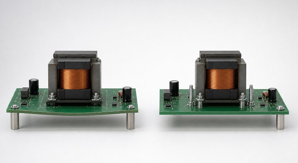
Greater thickness usually provides more bending stiffness when board material, dimensions, and mounting conditions remain unchanged.
However, mounting points, cutouts, and supports may improve rigidity without forcing a thicker overall construction.
Review vibration, dropping, shock, connector insertion loads, and unsupported areas during mechanical validation and product testing.
6.5. Why Should Your Connector Control PCB Thickness?
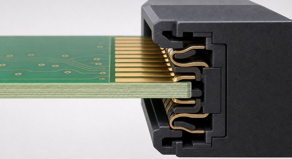
Thickness needs tighter control when a PCB enters card-edge connectors, as published manufacturer dimensions demonstrate.
Connector Example | Published Card or PCB Thickness |
Accepted card thickness: 1.57 mm; recommended range: 1.57–2.36 mm | |
Edge-card thickness: 1.57 mm; recommended PCB thickness: 1.60 mm | |
Accepted card thickness: 0.062 inch or 1.60 mm |
Use these examples only as context, then inspect the exact connector drawing before releasing fabrication files.
6.6. Does Thickness Change Your Controlled Impedance?
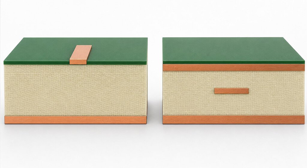
Trace impedance mainly follows dielectric thickness, dielectric constant, copper thickness, trace width, and reference-plane geometry.
Additional finished thickness never improves impedance automatically, so define the stackup before calculating transmission-line dimensions.
Request impedance coupons whenever your signal standard, customer specification, or internal quality plan requires physical verification.
6.7. Does a Thicker PCB Carry More Current?
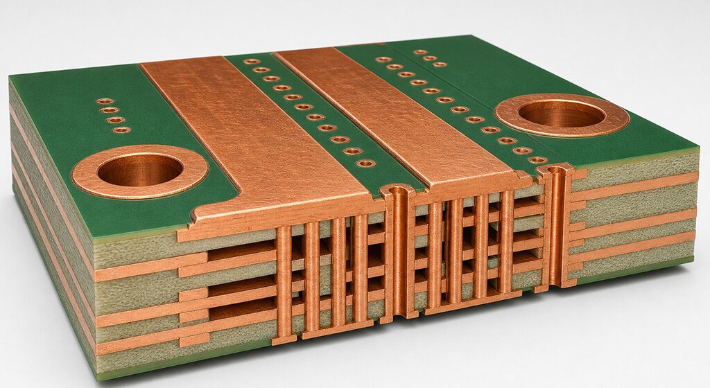
Extra FR-4 beneath conductors does not raise current capacity, because copper geometry and temperature control dominate.
Reference IPC-2152 when your process needs conductor-current guidance, while noting IPC no longer maintains this document.
Demanding power circuits still require careful calculations, thermal testing, environmental assumptions, and suitable engineering margins.
6.8. Does a Thicker PCB Improve Thermal Performance?
Examine the complete heat path because heavy copper, thermal vias, metal cores, heat sinks, or airflow may dominate.
Additional low-conductivity FR-4 can impede heat movement between sources and sinks instead of improving performance.
Consider an aluminum PCB when the application requires a dedicated metal base and controlled thermal path.
6.9. How Does Thickness Affect Drilling and Via Reliability?
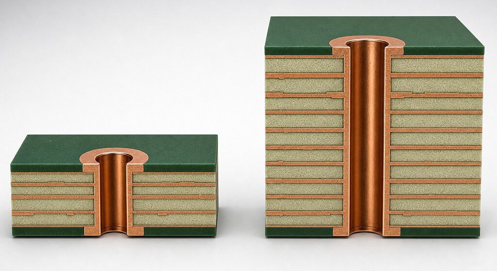
A thicker PCB increases drilling depth and via aspect ratio, making cleaning, activation, and copper plating harder.
Discuss small holes, thick boards, and reliability classes because difficult ratios may require larger vias or sequential lamination.
6.10. How Does Your Thickness Choice Affect Cost?
Stocked materials and mature stackups usually cost less than ultra-thin handling, deep drilling, or specialized laminates.
Compare complete product value, then request early fabrication review before expensive stackup or routing changes become necessary.
7. How Should You Handle Special PCB Types?
Rigid FR-4 assumptions can mislead designers using flex, rigid-flex, metal-core, or HDI constructions because each behaves differently.
7.1. How Should You Select Flex PCB Thickness?
Select flex thickness through bend radius, cycling demands, copper type, coverlay, layer count, and stiffener locations.
Connector zones often need local stiffeners, while active bending regions must remain thin enough for repeated movement.
Review PCBSAIL flex PCB capabilities whenever your design requires controlled static bending or repeated dynamic flexing during service.
7.2. How Should You Select Rigid-Flex Thickness?
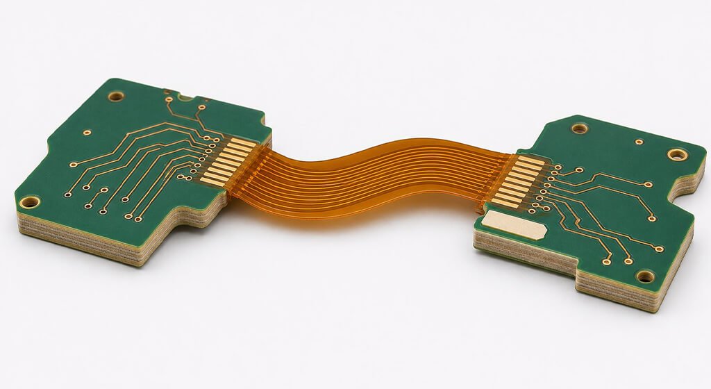
A controlled drawing must define thickness, transitions, coverlay, adhesives, stiffeners, and dimensions across every rigid-flex region.
7.3. How Should You Select Aluminum PCB Thickness?
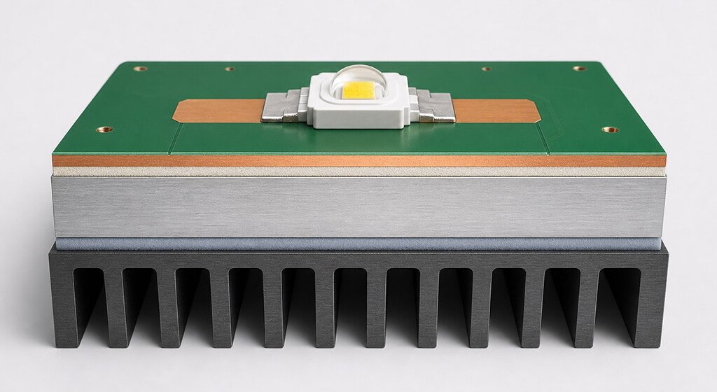
Keep aluminum base, dielectric, copper, and finished thickness separate, then select each value through product requirements.
Review PCBSAIL aluminum PCB capabilities before locking the metal-base stackup, insulation layer, and intended thermal path.
7.4. How Should You Select HDI Thickness?
Build HDI thickness around microvias, thin dielectrics, sequential laminations, fine traces, and restricted routing space.
HDI may reduce total profile, although fabrication becomes more complex than conventional multilayer board production.
8. How Should You Specify Thickness in Your Fabrication Notes?
Never specify only **standard thickness**, because fabricators need enough information for construction, inspection, and traceable documentation.
Adapt the following example inside fabrication drawings or procurement packages before approving any final production release.
FINISHED BOARD THICKNESS: 1.60 mm
FINISHED THICKNESS TOLERANCE: [APPROVED VALUE]
LAYER COUNT: 4
BASE MATERIAL: FR-4, Tg [APPROVED VALUE]
OUTER COPPER: [APPROVED VALUE]
INNER COPPER: [APPROVED VALUE]
CONTROLLED IMPEDANCE: YES/NO
FABRICATOR STACKUP APPROVAL REQUIRED BEFORE PRODUCTION: YES
Replace every bracketed value after engineering review, then document connector zones, buildup, edge thickness, and measurement locations.
Request first-article inspection whenever PCB thickness forms a critical tolerance chain inside your assembled product.
9. What Should You Confirm Before Requesting a Quote?
Send Gerber, drill, outline, layer, and drawing files alongside material, copper, thickness, tolerance, finish, and quantity requirements.
Request early stackup review because late dielectric changes can force complete impedance-controlled trace-width revisions across routed layers.
Use this compact checklist before requesting a formal PCB manufacturing quotation from any qualified fabricator:
- Finished PCB thickness and permitted tolerance
- Base material, glass-transition temperature, and flammability requirement
- Layer count, approved stackup, and impedance targets
- Starting and finished copper requirements
- Overall dimensions, panel restrictions, and controlled-depth features
- Surface finish, solder-mask requirements, and special coatings
- Connector zones, press-fit holes, and measurement locations
- Prototype quantity, production volume, and inspection expectations
10. FAQ About PCB Thickness
How Thick Is a Two-Layer PCB?
Regular PCB production supports several two-layer thicknesses, including 0.6, 0.8, 1.0, 1.2, and 1.6 mm.
Choose the final value from enclosure, connector, mechanical, stackup, handling, and fabrication requirements considered together.
What Is the Standard Four-Layer PCB Thickness?
Many four-layer boards use 1.6 mm, although compact products often support 0.8 mm or 1.0 mm constructions.
Approve the production stackup before routing impedance-controlled signals because dielectric changes alter calculated trace dimensions.
What PCB Thickness Tolerance Should You Specify?
Select PCB thickness tolerance through mechanical fit, connector geometry, material behavior, inspection capability, and supplier limits.
Never assume one universal tolerance protects every construction, board size, and supplier with equal reliability.
Is a Thicker PCB Always Better?
Greater thickness improves rigidity, but it also increases weight, drilling difficulty, material use, and sometimes cost.
Choose only the finished thickness genuinely justified through complete mechanical, electrical, assembly, and reliability requirements.
Does a Thicker PCB Carry More Current?
Greater finished board thickness does not automatically increase current capacity across copper traces or power planes.
Size copper weight, trace width, temperature rise, airflow, and cooling paths together as one thermal system.
What Is Your Best Starting Point?
Begin near 1.60 mm when a conventional rigid FR-4 design has no special mechanical or electrical restrictions.
Then verify connectors, enclosure dimensions, mechanical loads, stackup geometry, hole ratios, tolerance, and fabrication capability.
A complete product review produces better results than copying one familiar thickness from an unrelated design.
Contact PCBSAIL through its PCB manufacturing service when you need an experienced stackup review before quoting or production release.
11. Which Engineering Sources Support Your Decisions?
These primary documents support unit conversions, material ranges, foil terminology, connector examples, and rigid-board performance discussions.
- IPC Standards and Revision Status
- IPC-6012F: Qualification and Performance Specification for Rigid Printed Boards
- IPC-4101E-WAM1: Base Materials for Rigid and Multilayer Printed Boards
- IPC-4562B: Metal Foil for Printed Board Applications
- NIST Guide to SI Conversion Factors
- Isola 370HR Laminate and Prepreg Data Sheet