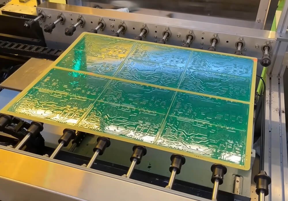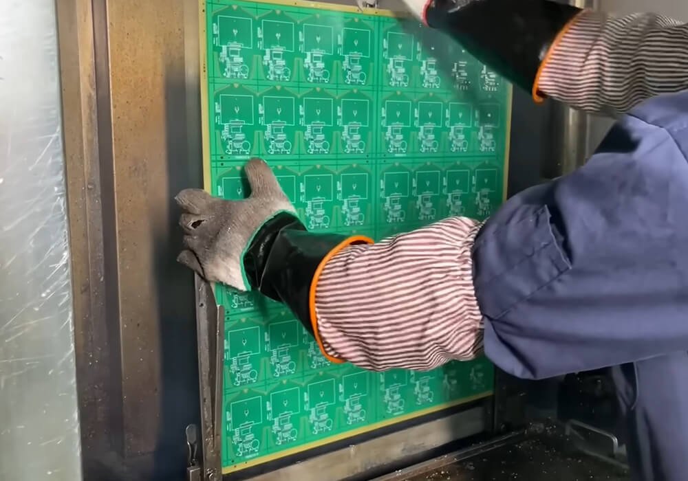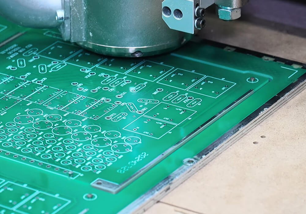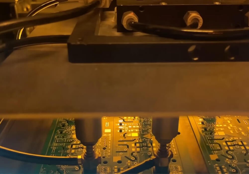
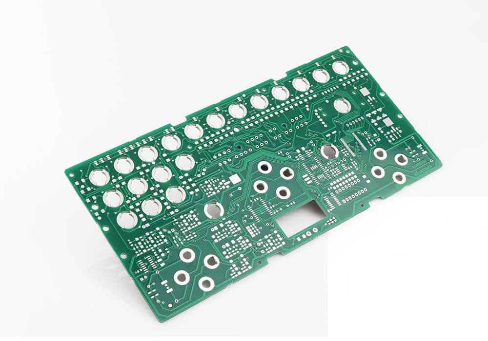
/From Prototype to Massive Production/
PCB Manufacturing Built Around Your Design.
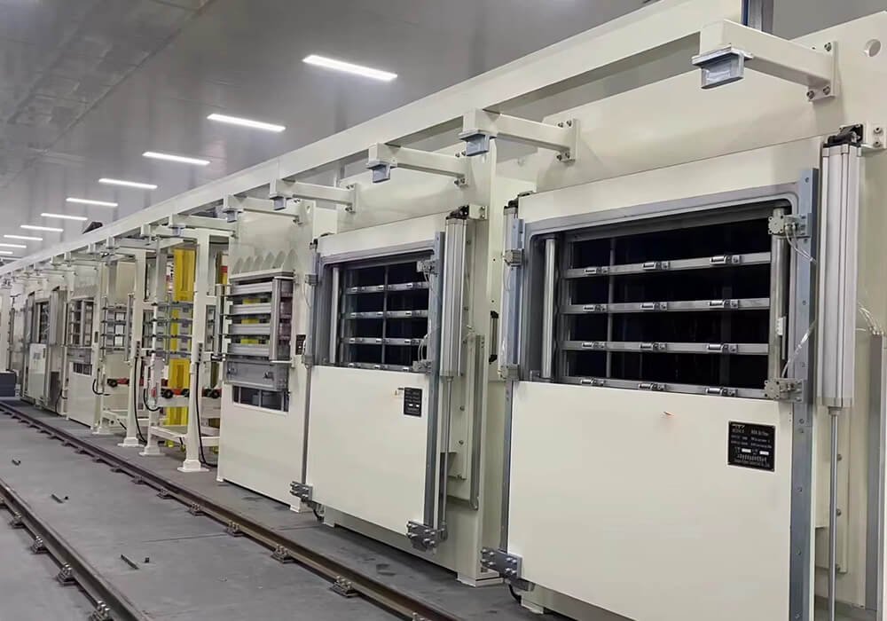
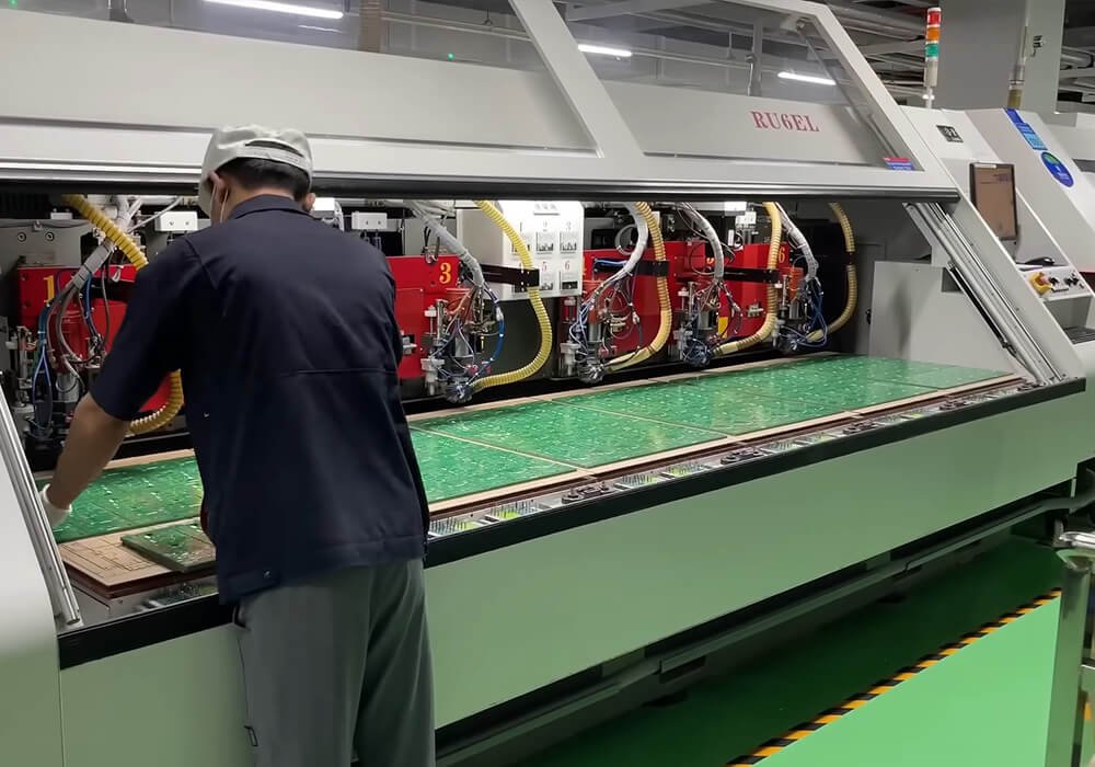
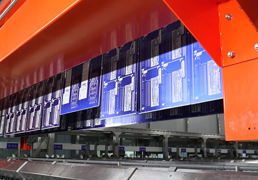
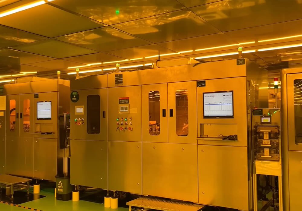
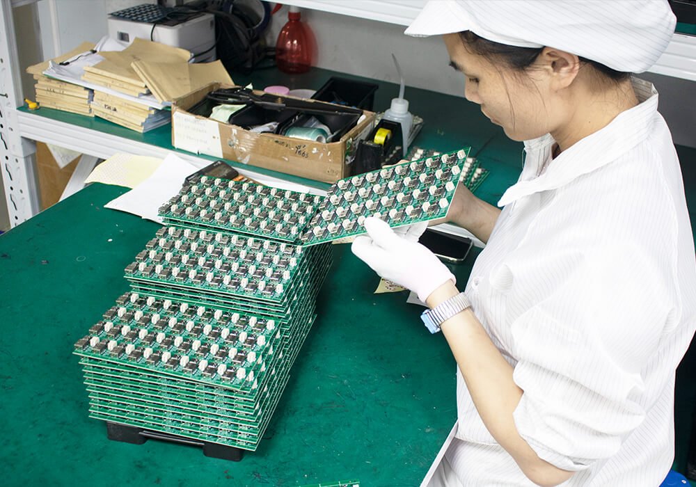
PCBSAIL supports PCB manufacturing from early prototypes through repeat production for engineering teams, startups, and established manufacturers.
Our engineers review your files, confirm practical limits, and define testing requirements before approved production begins.
±10% Impedance Tolerance
24h Fastest Prototype Build
Board Constructions Matched To Real Applications.
Every project is reviewed against its material, layer count, copper, thickness, geometry, and reliability requirements.
Rigid PCB use solid laminate structures that maintain their shape throughout assembly, installation, and normal operation.
It provided stable mechanical support for industrial controls, consumer devices, communications equipment, and power electronics.
Flexible PCB use polyimide-based structures that bend around tight spaces, moving parts, and compact product enclosures.
They can reduce wiring, connector counts, assembly weight, and packaging space when movement or folding is required.
Rigid-flex PCB combined rigid and flexible layers in one integrated circuit board.
It reduces connectors and cable assemblies while supporting three-dimensional packaging, repeated movement, and demanding installation layouts.
PCB Technologies We Manufacture
We support standard builds and specialized boards without forcing every project into one production model.
Multilayer PCBs are one of the most widely used PCB technologies for advanced electronic products.
It combined signal, power, and ground layers within compact layouts requiring controlled electrical performance.
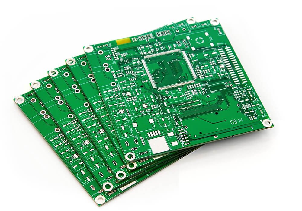
Our HDI PCBs use microvias and fine features to support dense routing around advanced component packages. They are designed for applications that requires compact size and high performance.
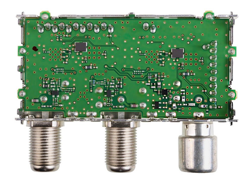
Our High-frequency PCB is made of Rogers laminate or PTFE materials. It can transfer the predictable radio-frequency signal across demanding applications.
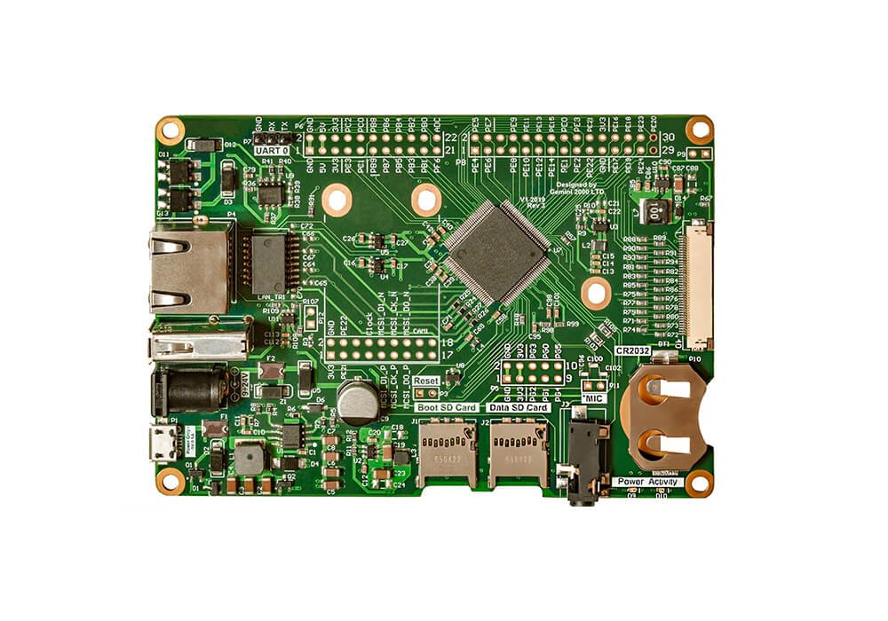
Our high-speed PCBs can offer signal integrity in fast digital systems.
It require planned stack-ups, controlled impedance, return paths, and suitable low-loss laminate systems for reliable operation.
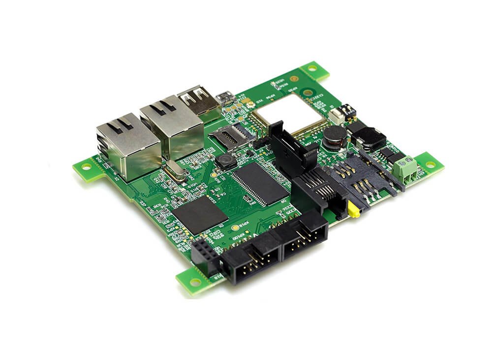
Our High Tg PCBs are engineered to withstand elevated thermal loads, providing superior reliability and long-term performance in high-temperature applications.
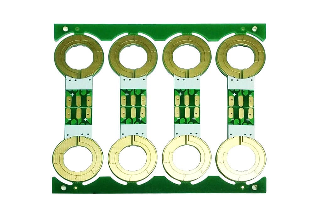
Heavy Copper PCBs are designed to carry higher currents while delivering superior thermal management for demanding power electronics and high-reliability applications.
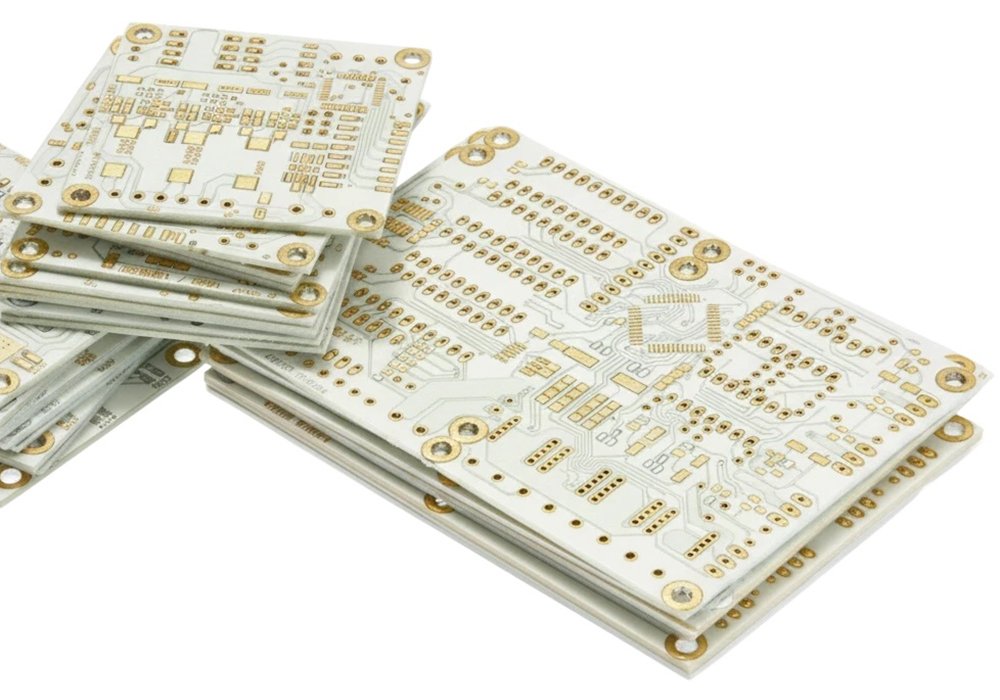
Our Ceramic PCB can deliver exceptional thermal conductivity, excellent electrical insulation, and outstanding reliability for high-power, RF, LED, automotive, aerospace, and industrial electronics.
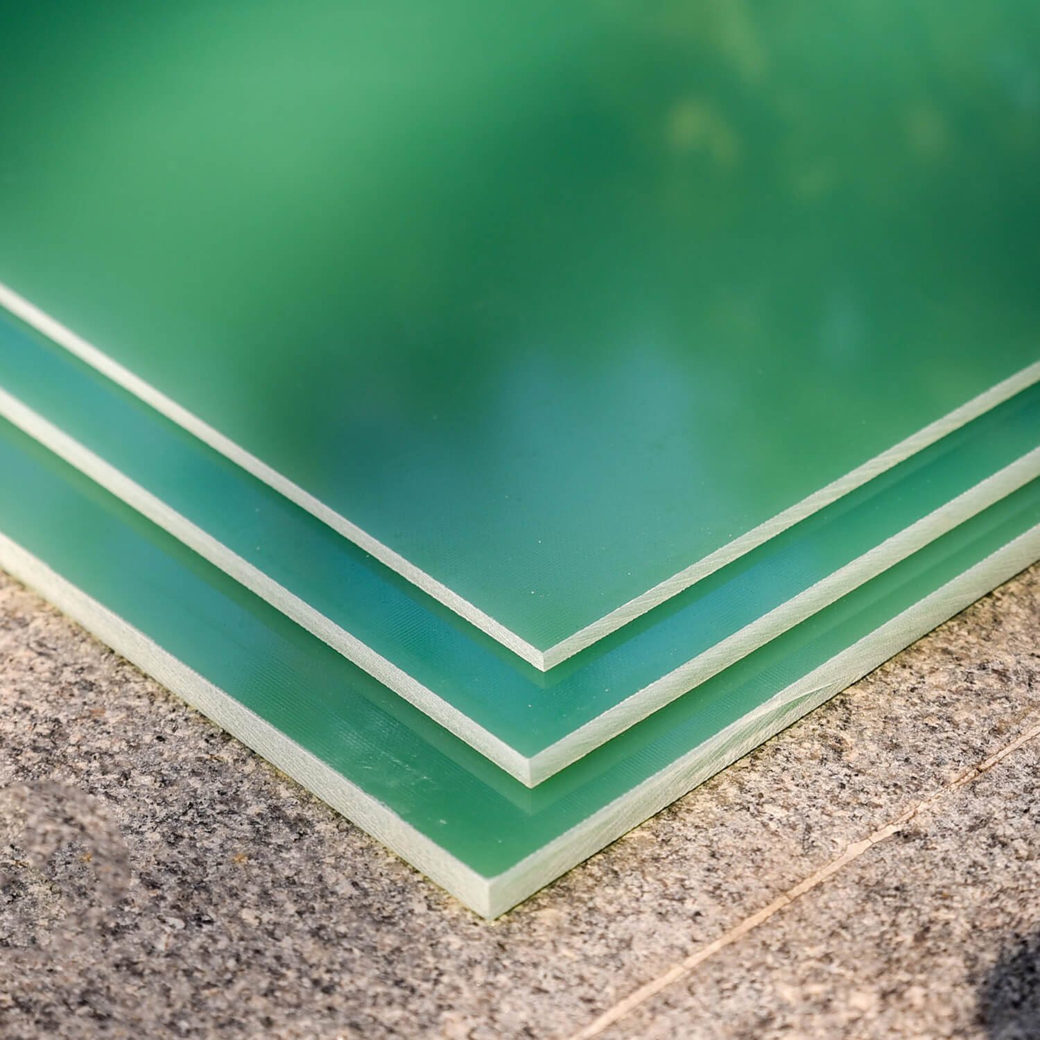
Our PCB Assembly Capability
It provides an initial reference for engineers comparing materials, structures, tolerances, and production options.
These values reflect published limits, while final capability depends on materials, thickness, dimensions, and order volume.
Capability | Production | Capability | Production |
Layer Count | 2–32 Layers | Min. Inner Trace / Space | 2.0 / 2.0 mil |
Board Thickness | 0.20–3.50 mm | Min. Outer Trace / Space | 2.5 / 2.5 mil |
Max. Board Size | 800 × 600 mm | Controlled Impedance Tolerance | ±8% |
Copper Thickness | 0.33–6 oz | Through-Hole Aspect Ratio | 12:1 |
Min. Mechanical Drill | 0.150 mm | Surface Finishes | HASL, Lead-Free HASL, ENIG, ENEPIG, OSP, Immersion Tin, Immersion Silver |
Min. Laser Drill | 0.100 mm | Standard | IPC Class 2 / Class 3 or Customer Specification |
What Should You Send?
- 1. Gerber or ODB++ fabrication files
- 2. Fabrication drawing and dimensions
- 3. Stack-up and impedance requirements
- 4. Material and surface finish requirements
- 5. Quantities, testing, and delivery needs
PCB Materials
PCB material defines the PCB’s Electrical Performance, Thermal Performance, Mechanical Reliability, and Manufacturing Cost. We will purchase the high-quality materials from verified suppliers to ensure PCB performance.
1. FR-4
FR-4 is the most widely used PCB substrate material worldwide. It is a fiberglass-reinforced epoxy laminate.
It can offer
- Cost Effective: FR-4 provides excellent performance at a competitive cost.
- Easy Manufacturing: Most PCB manufacturers have extensive experience processing FR-4 materials.
- Good Mechanical Strength: The fiberglass structure provides excellent rigidity and durability.
- Wide Availability: FR-4 materials are available in many thicknesses and grades.
2. High Tg FR-4
High Tg FR-4 is an enhanced version of traditional FR-4 designed for improved thermal reliability. It maintains mechanical stability at higher operating temperatures.
High Tg FR-4 Provides:
- Better Thermal Resistance
- Improved Dimensional Stability
- Reduced Thermal Expansion
- Higher Reliability
3. Rogers
Rogers are widely used for high-frequency and microwave applications.
Compared with standard FR-4, Rogers materials provide:
- More Stable Dielectric Properties
- Lower Signal Loss
- Better Frequency Performance
Popular Rogers Materials Include:
- Rogers RO4003C
- Rogers RO4350B
- Rogers RT/duroid series
4. PTFE
PTFE (Polytetrafluoroethylene) is a high-performance dielectric material used in demanding RF applications. It provides extremely low electrical loss.
PTFE offers:
- Very Low Dielectric Loss
- Excellent High-Frequency Performance
- Stable Electrical Characteristics
5. Metal Core
Metal Core PCBs use a metal base layer to improve thermal management.
Common Metal Cores Include:
- Aluminum
- Copper
Metal Core PCB provides:
- Excellent Heat Dissipation
- Better Mechanical Strength
- Improved Thermal Reliability
6. Ceramic
Ceramic are advanced materials designed for extreme thermal and electrical applications.
Common Ceramic Substrates Include:
- Aluminum Oxide (Al₂O₃)
- Aluminum Nitride (AlN)
- Silicon Carbide (SiC)
Ceramic PCBs provide:
- Excellent Thermal Conductivity
- High Temperature Resistance
- Low Thermal Expansion
- Long-Term Reliability
From Design Data To Inspected Bare Boards.
PCB Manufacturing Process
Our PCB manufacturing process goes through multiple precision manufacturing stages to transform design files into finished circuit boards
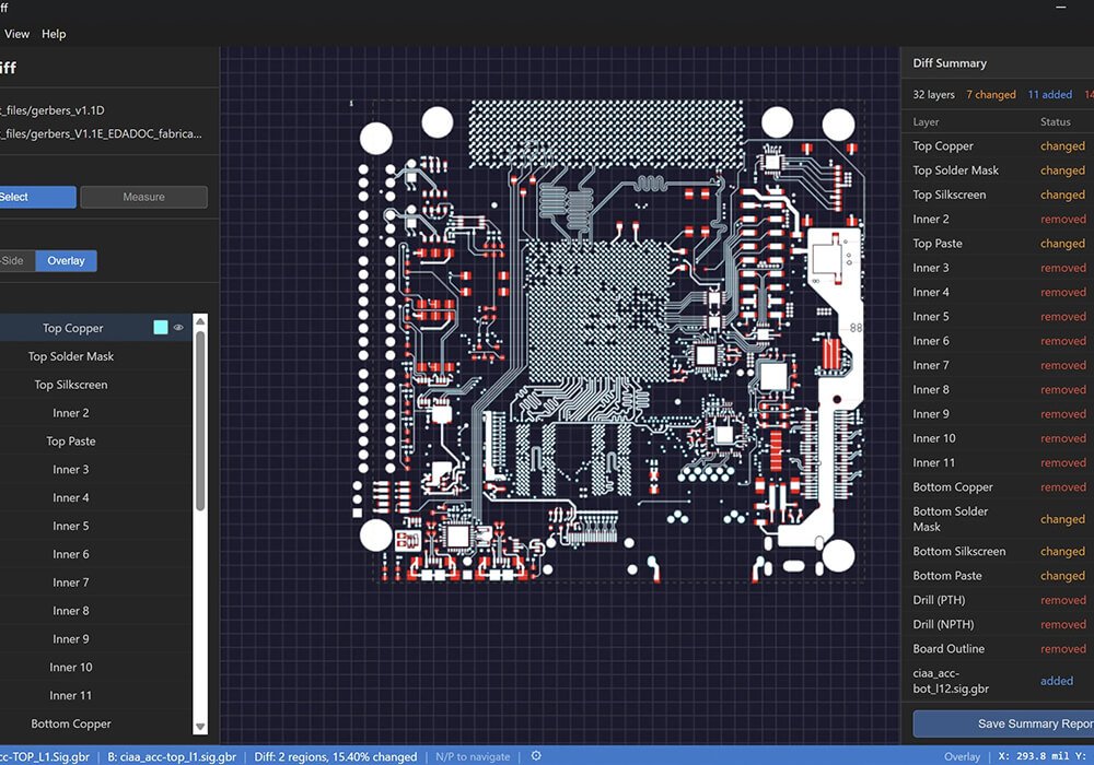
1. Engineering Review
Before manufacturing begins, our PCB engineers analyze the customer’s design files to ensure the PCB can be produced reliably.
We will review:
- Gerber Files
- Excellon Drill Files
- PCB Layer Stack-Up Information
- Fabrication Drawings
- Netlist Files
- Bill Of Materials (For PCBA Projects)
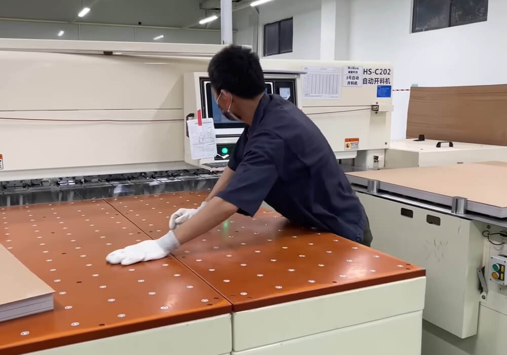
2. Material Preparation
After design approval, PCB production begins with material preparation. After confirming the PCB material, we will process these materials.
Typical PCBs are composed of :
- Copper Foil: Provides electrical conductivity.
- Dielectric Layer: Provides insulation between copper layers.
- Core Material: Provides mechanical strength.
- Prepreg: A bonding material used during lamination.
3. Inner Layer Imaging Copper Surface
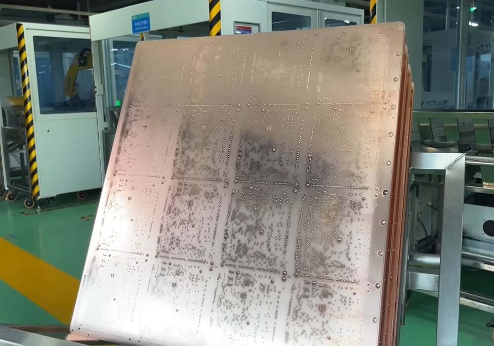
Copper surfaces are cleaned to remove:
- Oxidation
- Dust
- Contamination
A clean surface ensures proper photoresist adhesion.
4. Inner Layer Imaging Circuit Pattern Exposure
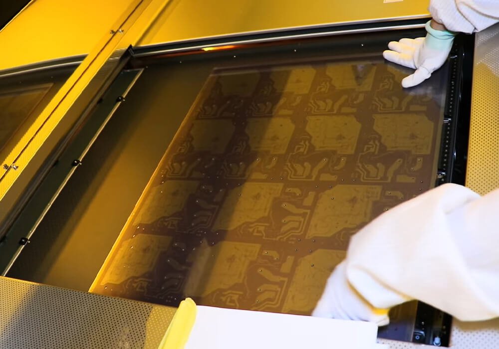
The PCB artwork is transferred onto the photoresist using:
- Laser Direct Imaging (LDI)
- Photolithography systems
The exposed areas define the circuit pattern.
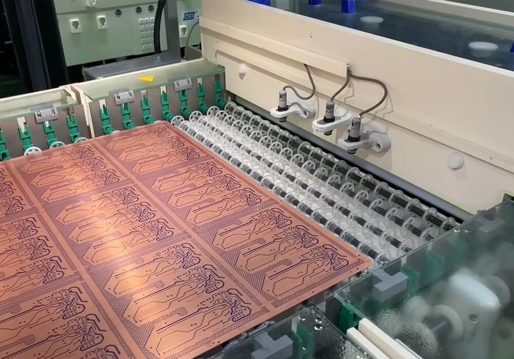
5. Inner Layer Etching
After imaging, unwanted copper is removed through chemical etching. The process creates the actual circuit pattern.
Etching Process
- Protected copper remains
- Exposed copper is removed
The result is a precise inner-layer circuit.
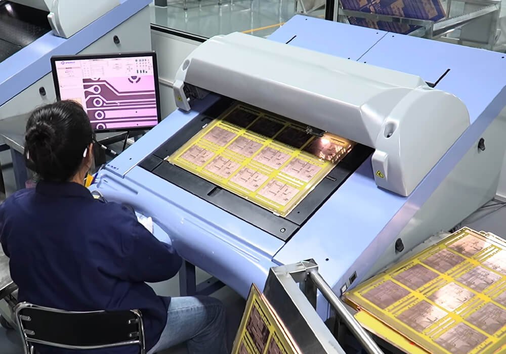
6. Inner Layer AOI Inspection
After etching, inner layers undergo Automated Optical Inspection. AOI systems compare the manufactured PCB layer with the original design database.
AOI Detects:
- Missing Traces
- Extra Copper
- Short Circuits
- Broken Circuits
- Pattern Defects
- Alignment Errors
AOI inspection is critical because inner-layer defects become impossible to repair after lamination.
7. Layer Lamination
Multilayer PCB manufacturing requires bonding multiple layers into one solid structure.
- Lamination Process Steps 1. Layer Alignment
All PCB layers are precisely aligned using optical targets. High accuracy is required because even small alignment errors can affect via connections and signal performance.
- Lamination Process Steps 2. Heat and Pressure Application
The stacked PCB layers are placed into a lamination press to create a permanent bond.
8. CNC Drilling Process
After lamination, holes are drilled into the PCB.
PCB drilling creates:
- Through holes
- Via holes
- Component mounting holes
9. Copper Plating Process
After drilling, hole walls are not conductive. Copper plating creates electrical connections between PCB layers.
- Plating Steps 1. Chemical Copper Deposition
A thin copper layer is deposited onto hole walls and PCB surfaces.
- Plating Steps 2.Electrolytic Copper Plating
Additional copper thickness is added to improve current carrying capability and mechanical reliability.
10. Outer Layer Imaging and Etching
The outer layer imaging and etching is one of the most critical stages in PCB manufacturing. It creates the external copper circuit patterns that connect electronic components, connectors, and other electrical elements on the finished printed circuit board.
It Includes:
- Photoresist Coating
- Circuit Imaging
- Copper Plating
- Etching
- Inspection
11. Solder Mask
The solder mask is a protective coating applied over the PCB surface. It is commonly recognized as the green layer covering most PCBs.
Solder mask provides:
- Prevents copper oxidation and environmental damage.
- Prevents accidental short circuits.
- Prevents solder bridges during assembly.
Common Solder Mask Colors
- Green
- Black
- Blue
- Red
- White
- Yellow
The color choice usually depends on customer preference.
12. Surface Finish
The exposed copper pads require protection before component assembly. Surface finish improves solderability, corrosion resistance, and storage life.
Common PCB Surface Finishes
13. PCB Cutting and Profiling
After surface finishing, individual PCBs are separated from production panels.
Methods Include:
- CNC routing
- V-scoring
- Laser cutting
14. Electrical Testing
Before shipment, finished PCBs undergo flying probe testing.
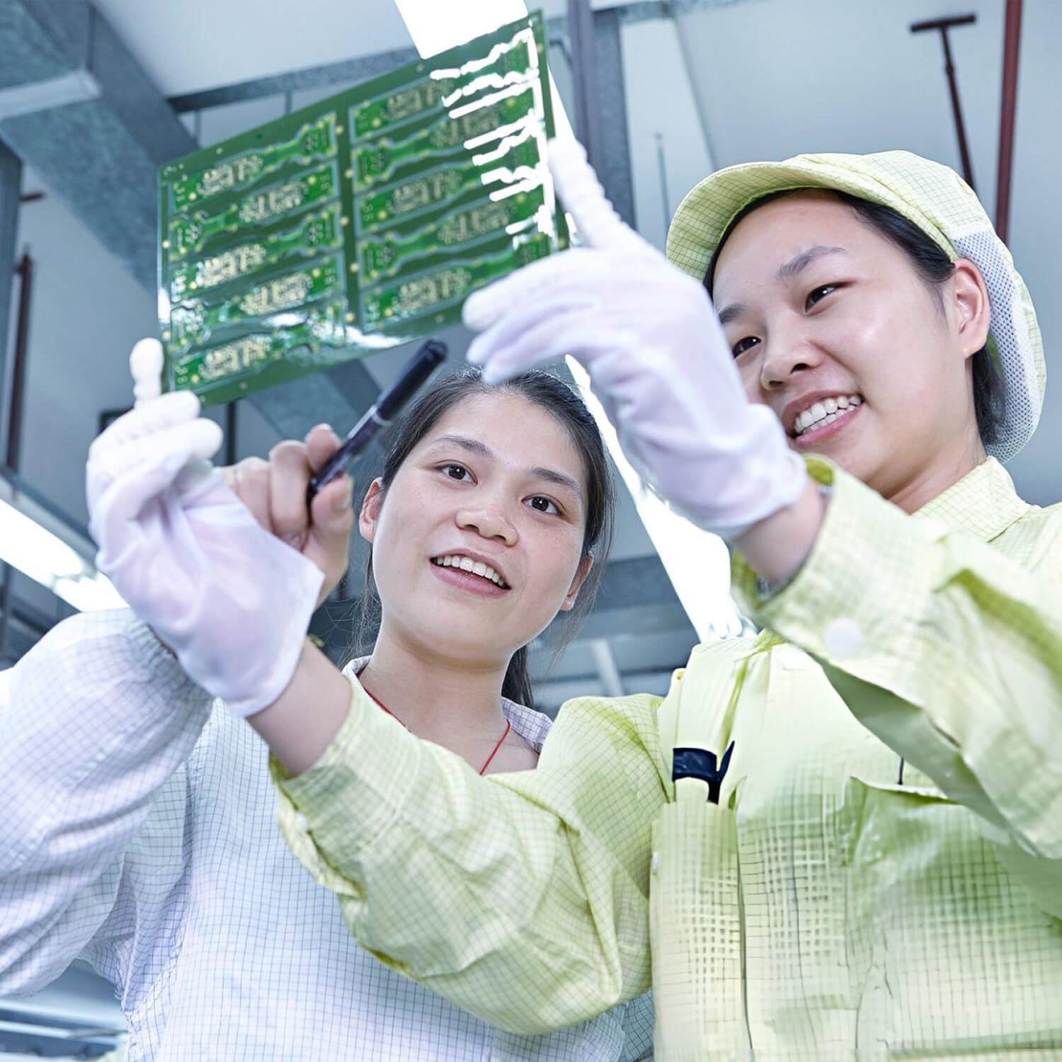
15. Final PCB Inspection
The final quality inspection ensures that every PCB meets customer specifications.
Our inspection teams verify:
- PCB Appearance
- Hole Quality
- Surface Finish
- Marking Accuracy
- Quantity
16. Packaging
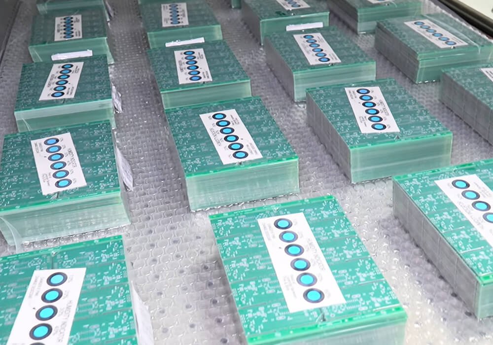
After passing inspection, PCBs are packaged carefully.
We will pack it with:
- Vacuum sealing
- Moisture barrier bags
- Protective packaging materials
PCBs are then shipped to customers worldwide.
Quality Control and Testing
Quality control should verify measurable requirements at appropriate stages instead of relying on final visual inspection alone.
Testing methods are selected according to board structure, order volume, reliability needs, and customer-approved acceptance criteria.
1. Incoming Material Inspection
All laminates, copper foil, solder mask, and other raw materials are verified for identity, quality, and condition before entering production.
2. Inner Layer AOI Inspection
Hole dimensions, registration accuracy, and copper plating quality are inspected to ensure reliable electrical interconnections.
3. Electrical Testing
Every finished PCB undergoes electrical testing to verify circuit continuity, isolation, and compliance with the approved netlist.
4. Controlled Impedance Verification
For impedance-controlled designs, Time Domain Reflectometry (TDR) testing confirms that impedance values meet the specified tolerances.
5. Final Quality Inspection
Before shipment, each order is inspected for board dimensions, surface finish, solder mask, silkscreen, hole quality, packaging, labeling, and quantity to ensure it fully complies with customer requirements.
Industries We Offered
We offer custom PCB manufacturing solutions for a wide range of industries, from consumer electronics to mission-critical aerospace systems.

Automation
Industrial PCBs must deliver stable performance in demanding environments. We support applications that require high durability, power handling, and long operating life.
- PLC Controllers
- Industrial Robots
- Servo Drives
- Motor Controllers
- Automation Equipment
Automotive Electronics
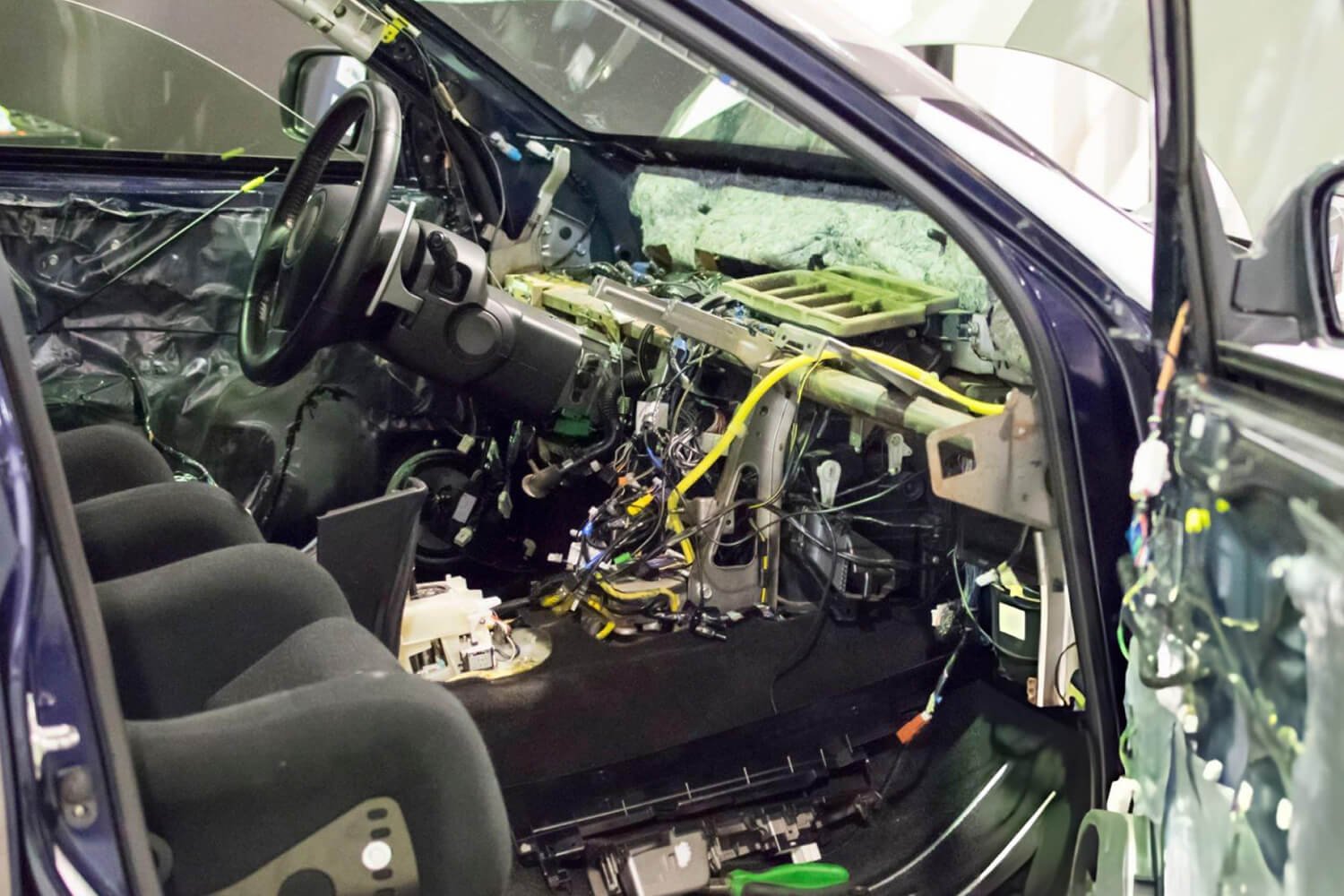
We offer automotive-grade PCBs designed to withstand harsh operating conditions, including high temperatures, vibration, and continuous operation.
- Battery Management Systems (BMS)
- EV Chargers
- ADAS Modules
- Engine Control Units (ECU)
- Automotive Lighting Systems

Consumer Electronics
We manufacture high-volume, cost-effective PCBs for modern consumer products, supporting compact designs, rapid production cycles, and consistent quality.
- Smartphones
- Tablets
- Laptops
- Smart Home Devices
- Wearable Electronics

Renewable Energy
Our PCBs support the growing renewable energy market with high-power, thermally optimized circuit boards.
- Solar Inverters
- Energy Storage Systems (ESS)
- Wind Turbine Controllers
- EV Charging Stations

Medical Electronics
Medical equipments requires strict quality management, traceability, and high manufacturing precision. Our PCB can support reliable operation for critical healthcare devices.
- Diagnostic Equipment
- Patient Monitoring Systems
- Medical Imaging Devices
- Portable Healthcare Equipment
Telecommunications
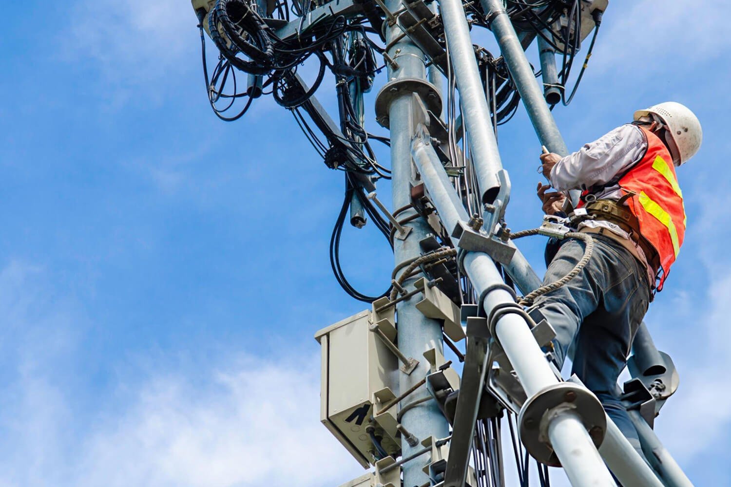
High-speed communication systems require precise impedance control and low-loss materials. Our RF and high-frequency PCBs were made from premium laminates such as Rogers and PTFE.
- 5G Infrastructure
- RF Modules
- Wireless Communication Equipment
- Satellite Communication Systems
Fast Quotation
Our professional sales and engineering teams provide fast PCB quotes and technical support. Simply send us your Gerber files, BOM, and assembly drawings, and we will respond promptly with a competitive solution.
- Gushu Tangxi Second Industrial Zone, Shenzhen
- +86 755 2335 0814
- +86 135 1078 8094
- sales@pcbasail.com
FAQ About PCB Manufacturing
1. What Affects PCB Manufacturing Cost?
PCB manufacturing cost depends on materials, layer count, dimensions, copper weight, feature sizes, finishes, testing, and quantity.
Tighter tolerances and uncommon materials usually add process steps, reduce panel efficiency, or increase procurement risk.
Early engineering review often identifies practical changes that reduce cost without weakening the product’s required performance. Provide complete files and realistic quantities so the quotation reflects actual requirements instead of broad assumptions.
2. What Affects PCB Manufacturing Lead Time?
Lead time depends on material availability, board complexity, tooling, testing, order volume, and the requested delivery schedule.
Standard materials and established design rules generally move faster than uncommon laminates or complex sequential constructions.
Production begins only after technical questions, commercial terms, and released manufacturing documentation receive written approval.
Ask for separate fabrication and shipping dates when your project has a fixed laboratory or production deadline.
3. Can PCBSAIL Manufacture Prototype Boards?
Prototype builds help engineering teams verify function, dimensions, assembly fit, and manufacturability before larger production commitments.
4. What Is The Difference Between PCB Manufacturing And PCB Assembly?
PCB manufacturing creates the bare circuit board, while PCB assembly mounts and solders components onto that board.
5. How Many PCB Layers Can You Manufacture?
1-32 Layers. Layer capability depends on materials, thickness, via structure, dimensions, tolerances, order volume, and inspection requirements.
6. What Surface Finishes Are Available?
PCBSAIL offers multiple surface finishes:
- ENIG
- HASL / Lead-Free HASL
- OSP
- Immersion Silver
- Immersion Tin
All finishes are RoHS compliant and compatible with lead-free assembly.
7. Can You Manufacture Controlled-Impedance PCB?
Yes. We Can. Controlled impedance requires an approved stack-up, material data, target values, trace geometry, and defined test tolerances.