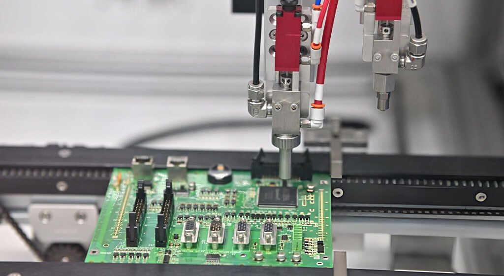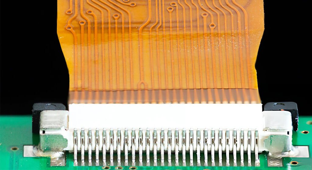

Rigid-flex PCB integrates rigid and flexible circuit sections into one printed circuit board. The rigid sections support components and mounting features. Flexible sections carry electrical connections and accommodate planned bending or folding.
Rigid-flex PCB design’s challenge is matching the electrical layout to the mechanical construction. Materials, copper thickness, and reference layers affect both signal performance and bending behavior.
This guide helps you define bending conditions, choose a stackup, and develop practical layout rules.
It also explains how to specify manufacturing requirements and verify the finished construction.
Key Takeaways:
- Bending conditions should be defined before material selection and routing.
- Finished flexible thickness includes every layer present in the bend.
- Active bend areas need controlled conductor geometry and carefully placed features.
- High-speed signals need suitable reference paths across regional transitions.
- Verification should address the actual assembly, movement, and service environment.
Table of Contents
1. What Is a Rigid-Flex PCB?
A rigid-flex printed circuit board (PCB) integrates rigid and flexible circuit sections into a single board. Its rigid sections support components, while flexible sections carry electrical connections and accommodate planned bending.
This construction lets you position connected sections on different planes and can replace selected cables or connectors.
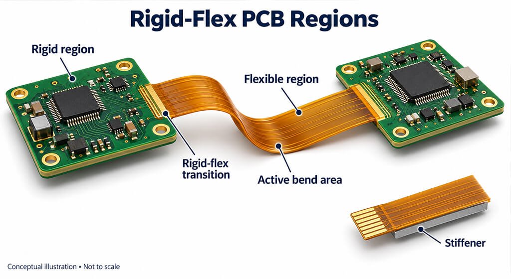
1.1. How the Board Regions Differ?
Your layout should distinguish the flexible material from the area expected to bend.
Region | Function | What the design should define |
Rigid Region | Supports components and mounting features | Outline, stackup, and attachment locations |
Flexible Region | Carries circuitry through flexible materials | Material construction and routing boundaries |
Active Bend Area | Deforms during installation or operation | Bend location, direction, radius, and movement |
Rigid-Flex Transition | Connects rigid and flexible constructions | Material boundaries and nearby clearances |
Stiffened Area | Provides local reinforcement | Support coverage and finished thickness |
A flexible region may contain stationary sections beside the active bend. Those sections can require reinforcement for connections or assembly. Bend-specific restrictions apply to the expected deformation area.
1.2. Rigid-Flex VS Other Interconnect Options
Your choice depends on available space, assembly access, and replacement needs.
Construction | When to consider it | Main tradeoff |
Integrated rigid-flex PCB | Connected sections need a compact, folded arrangement | Fabrication complexity and replacement of the integrated board |
Flexible printed circuit with stiffeners | A flexible interconnect needs supported terminations | Reinforcement placement and connector thickness |
Separate rigid boards joined through connectors | Boards or cables need independent replacement | Connector space, retention, and mating access |
A flexible printed circuit (FPC) can have bonded reinforcement beneath its termination. The reinforcement provides support.
The fabrication cross-section should be distinguished from that arrangement from an integrated rigid-flex multilayer construction.
2. Define the Bending Conditions Before Layout
The bending conditions determine the mechanical requirements for the flexible section.
Folding, maintenance, and continuous movement need different requirement on the construction.
Before routing, we need to map out the motion path, assess the available space, and determine the expected lifespan.
These factory affects material selection, bend geometry, and the the finished board test.
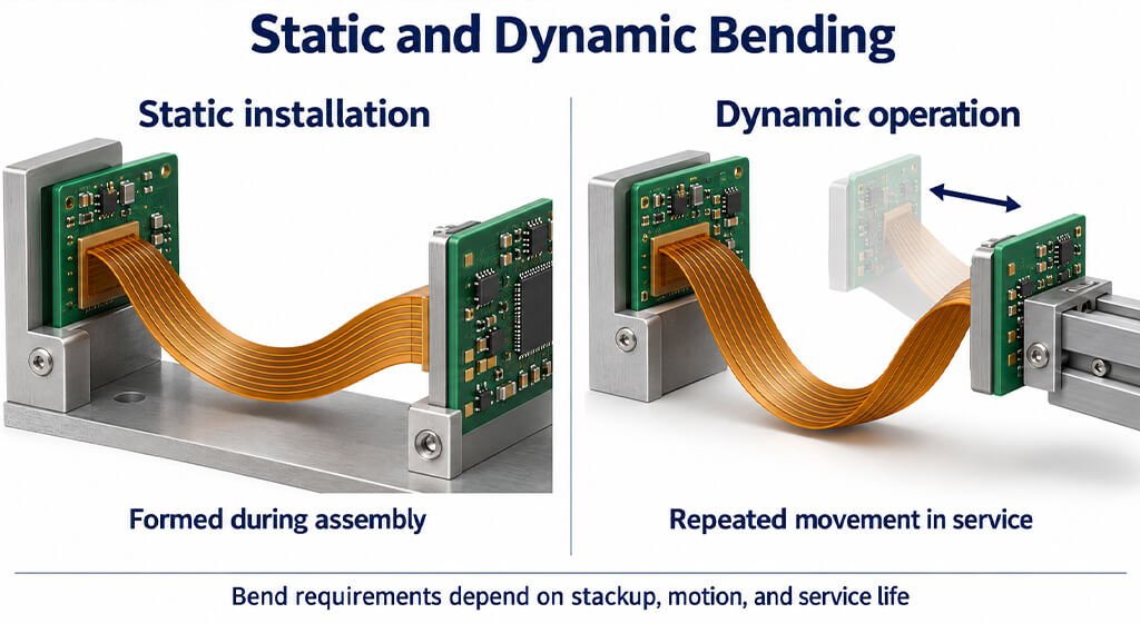
2.1. Static VS Dynamic Bending
A static flex section bends during installation and then remains substantially fixed. A dynamic flex section moves repeatedly during operation.
When it comes to maintenance bending, it’s important to think about it separately because it may change the bend location or direction.
Condition | Information needed | Verification focus |
Installation bending | Assembly path, angle, and installed shape | Forming and installation trials |
Maintenance bending | Access procedure and expected interventions | Representative service-cycle testing |
Dynamic bending | Motion, radius, speed, and required cycles | Endurance testing under defined conditions |
2.2. Build a Design Input Sheet
Your input sheet should describe the entire movement, including assembly and servicing.
Mechanical inputs include bend locations, angles, fixed points, and available clearances. We also need to consider twisting, rubbing surfaces, and insertion forces.
Electrical inputs include current, interface requirements, impedance targets, and permitted loss. The operating conditions are made up of temperature, humidity, and vibration.
If the motion path changes, we need to review the geometry before layout. A final folded image cannot show every condition experienced during installation.
3. How to Select Rigid-Flex PCB Materials?
The materials must meet bending, electrical, and assembly requirements together.
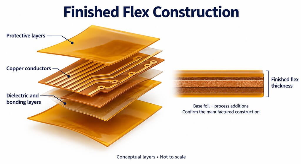
The substrate, copper, coverlay, and adhesive form a finished construction. Its thickness affects mechanical behavior. So we should should consider the proposed stackup and operating conditions when choosing material.
Before finalizing the layout, it’s a good idea to confirme the materials, the constructions with your PCB fabricator.
These factory affects material selection, bend geometry, and the the finished board test.
3.1. Flexible Base Materials
Polyimide (PI) is a common insulating substrate for flexible circuits.
Flexible copper-clad laminate (FCCL) are made of the dielectric material and copper foil.
Adhesive-based and adhesiveless laminates use different bonding constructions. It will affect finished thickness and processing requirements.
Other substrates are available. Panasonic documents flexible multilayer materials using liquid crystal polymer (LCP). Their suitability still depends on the application and construction.
FR-4 can be used in forming rigid regions. Your drawing should identify its function and keep it distinct from the intended flexible substrate.
3.2. Rolled-Annealed VS Electrodeposited Copper
When selecting the foil choice, we should account for thickness, processing, and expected movement.
Rolled-annealed (RA) copper is commonly considered for repeated bending. Electrodeposited (ED) copper is available in different grades.
Altium identifies RA copper and thinner copper constructions can improve bend life.
The finished conductor may also include plating.
3.3. Coverlay and Adhesive Selection
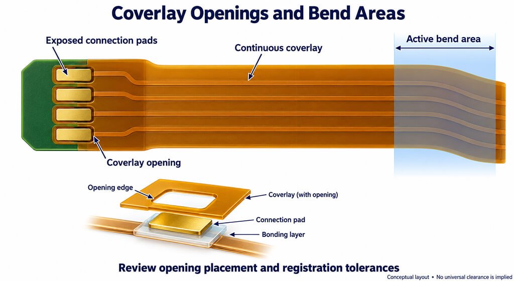
Coverlay is an insulating protective layer applied over flexible circuitry.
Openings expose pads and other electrical contact areas. Its thickness and adhesive will definds the flexible stackup.
Opening edges also create local changes in construction.
Your fabrication package should identify the material system and opening boundaries. Your supplier needs to confirm registration tolerances, bonding conditions, and adhesive flow.
Ordinary solder mask should not be replaced without checking compatibility with the intended movement.
3.4. Stiffener Selection and Position
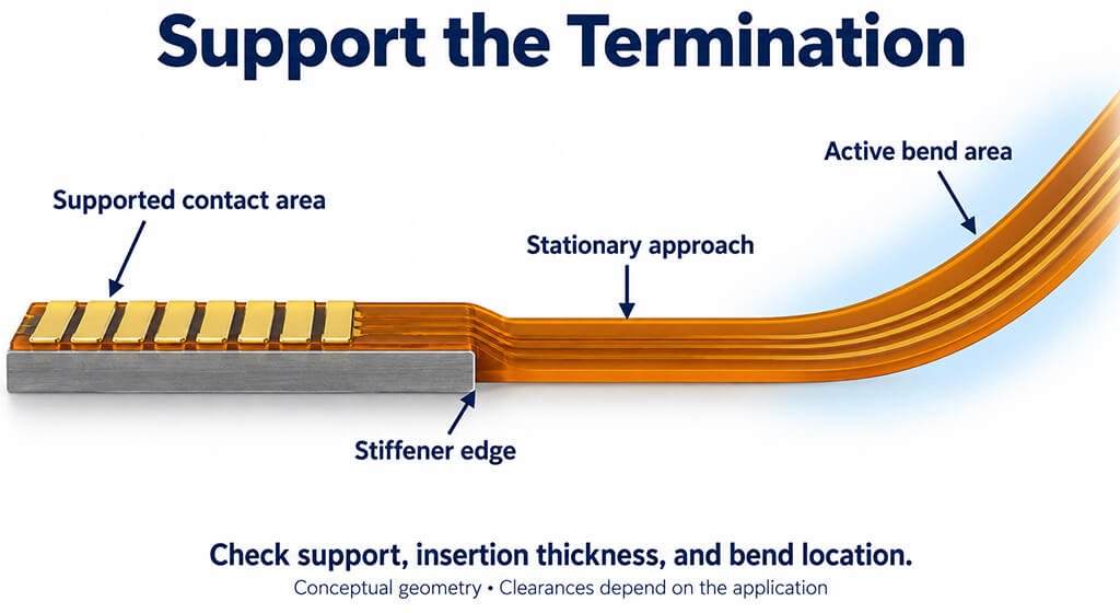
The stiffener should support a connection or assembly.
A component area may need to be reinforced during placement and soldering.
A connector tail may need a controlled insertion thickness.
All Flex describes FR-4/G10 and polymer stiffeners for these purposes. Its guide also explains how reinforcement supports components and connector terminations.
The edge introduces a stiffness transition. Its location needs to be reviewed against the expected bend and assembly tolerances.
4. How to Design the Rigid-Flex PCB Stackup?
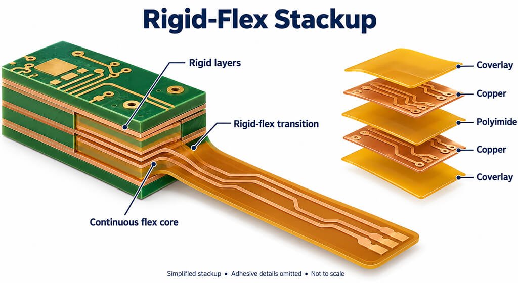
Your stackup should define the complete construction in every board region.
The flexible section needs sufficient routing and reference conductors without unnecessary thickness.
Rigid sections may use additional layers for component connections and power distribution.
4.1. Allocate Layers Between Rigid and Flexible Regions
The rigid-region layer count does not automatically determine the flexible layer count. The conductors and reference structures need to continue through the interconnect.
Decision | Mechanical Effect To Assess | Electrical Requirement To Preserve |
Flexible Layer Count | Thickness and stiffness | Routing capacity and reference paths |
Copper Thickness | Finished conductor behavior | Resistance and current capacity |
Dielectric Thickness | Bend thickness and conductor position | Impedance and coupling |
Copper Coverage | Local stiffness | Reference continuity and shielding |
Bonded Or Unbonded Layers | Relative movement during bending | Controlled spacing and coupling |
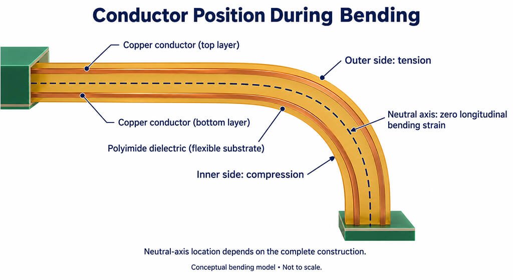
The neutral axis is the position through a bent section where longitudinal bending strain is approximately zero. Its location depends on the materials and their thicknesses.
Conductors closer to that axis generally experience less bending strain. Their positions must also support the intended electrical structure.
4.2. Design the Rigid-Flex Lamination Transition
The transition needs controlled material boundaries and a compatible bonding process.
Prepreg is resin-impregnated reinforcement used during lamination. Suitable low-flow or no-flow systems help control resin movement near flexible openings.
Glass styles such as 1080 and 2116 describe reinforcement construction. They do not independently specify resin chemistry or flow behavior.
Your drawing should identify the rigid-material edge, coverlay termination, and bonding boundaries.
4.3. Manage Changes in Layer Count
Your cross-section should show which layers continue into each flexible section.
A stepped construction may suit a particular design. Other boards use a defined rigid edge around a thinner flexible interconnect. The arrangement depends on the manufacturing process.
For multiple flexible layers, their relative lengths and bonding arrangement also matter. IPC-2223E identifies unbonded constructions and differential lengths as separate design topics. The directory confirms topic coverage, not specific design limits.
5. How to Determine Bend Radius and Flexible Length?
The bend radius and flexible length must suit the stackup and movement.
Radius determines the curvature, while length allows the circuit to follow the path. Both need clear measurement references.
Preliminary calculations help check available space, but the proposed geometry still needs fabrication review and representative testing.
5.1. Evaluate the Minimum Bend Radius
A common preliminary relationship is:
- R = kT
Here, R is the specified bend radius. T is the finished flexible thickness, and k depends on construction and operating conditions.
All Flex gives approximately R = 10T as a design guideline. It does not establish a universal dynamic-life guarantee.
Your drawing must identify the radius reference. An inside-surface radius differs from one measured along a conductor or neutral-axis path.
5.2. Calculate the Required Flexible Length
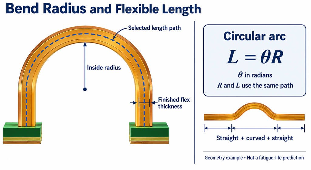
For an ideal circular path:
- L = θR
The angle θ uses radians. The radius must be same with the path used for the length.
For a 180° bend, the arc length is πR. Altium points the equivalent relationship using degrees in its bend-line geometry guidance.
Straight approaches, mounting positions, and assembly allowances increase total length. Excess length also needs control because an unsupported loop can buckle or contact nearby surfaces.
5.3. Work Through a Preliminary Example
The following inputs are assumed for a geometric example. They do not describe a qualified construction.
Suppose your preliminary inside radius is 1.0 mm. The finished flexible thickness is 0.10 mm. A separate mechanical assessment places the neutral axis 0.05 mm from the inside surface.
For a 180° bend:
- The neutral-axis radius is 1.0 + 0.05 = 1.05 mm.
- Its arc length is π × 1.05 ≈ 3.30 mm.
- Straight sections and agreed assembly allowances are added afterward.
- The complete path is checked against the enclosure and installation sequence.
The neutral-axis position is an explicit assumption in this example. It should not automatically be taken as half the thickness.
6. Component Placement and Regional Layout
Your components and mounting features should be placed where the board provides stable support.
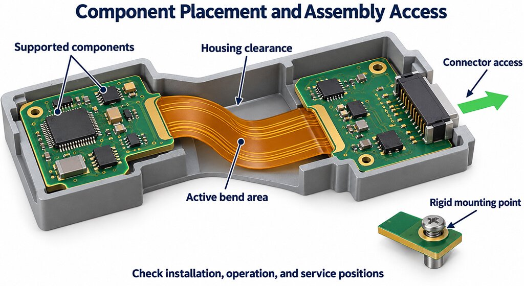
Large packages and connectors generally should be positioned in rigid regions. Supported, stationary flexible sections may also carry suitable components.
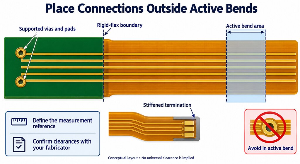
The active bend area needs separate keepout zone based on the expected movement, positional tolerances, and assembly loads.
6.1. Where Should Components Be Placed?
Rigid sections are usually preferable for heavy components and large packages.
Ball grid array (BGA) package and quad flat no-lead (QFN) packages need stable assembly support. Connectors also transfer insertion and handling forces into the board.
A stationary flexible section may accommodate components if its reinforcement and assembly process are suitable.
You should consider the support during manufacture and the loads after soldering when you are reviewing.
6.2. Which Features Need Bend-Area Keepouts?
Your keepout should cover the expected deformation envelope.
Feature | Main Concern | Placement Approach |
Components And Connectors | Attachment stiffness and external loading | Use rigid or supported stationary areas |
Vias And Plated Holes | Local structural changes | Move layer transitions outside active bending |
Pads And Test Points | Exposed copper and attached joints | Keep connections in supported areas |
Mounting Holes | Material interruption and applied loads | Separate them from the bend |
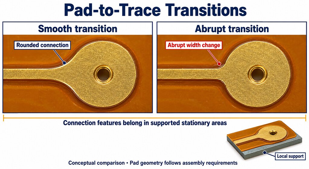
Abrupt Copper Features | Local geometry changes | Maintain smooth conductor paths |
A nominal bend line does not describe the entire curved area. Assembly variation may also move the actual bend beside that line.
6.3. Check Mounting and Assembly Access
Your mechanical review should follow the installation sequence. Electronic computer-aided design (ECAD) and mechanical computer-aided design (MCAD) models help check fit and access.
Altium describes their use in rigid-flex mechanical collaboration.
The review should cover:
- Mounting points and fixed regions.
- Connector insertion and removal.
- Intermediate positions during enclosure closure.
- Clearance from screws, ribs, and sharp edges.
- Movement required during servicing.
Physical assembly trials can reveal handling forces and unintended bending that a geometric model misses.
7. Bend-Area Routing Rules
Your conductors should pass smoothly through the active bend area with consistent geometry.
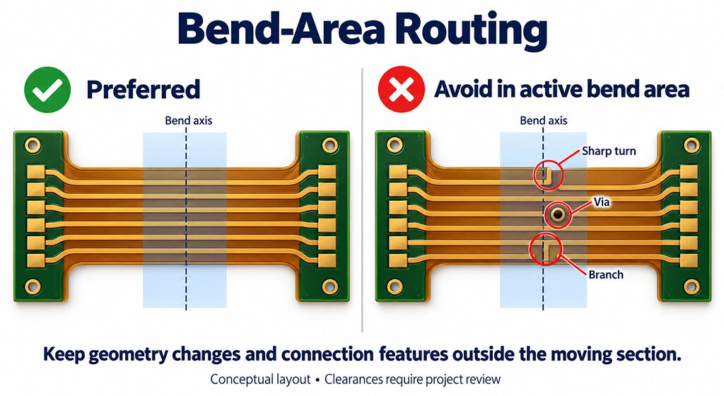
Traces generally cross the bend axis at right angles. Corners, branches, and width transitions are better placed outside the moving section.
Width and spacing must also satisfy electrical requirements, so the final layout needs to be reviewed against the complete stackup and operating conditions.
7.1. Align Conductors With the Bend Geometry
Your drawing should distinguish the bend axis from the direction of bending.
The axis runs along the fold, like a hinge line. Conductors generally cross it rather than following it.
Unnecessary turns should remain outside the deformation envelope. For double-sided constructions, opposing traces also need evaluation.
All Flex recommends staggered conductors rather than direct overlap to retain flexibility. Any change in layer alignment must preserve the required electrical geometry.
7.2. Select Trace Width and Spacing
The trace dimensions need to satisfy current, temperature rise, impedance, and manufacturing limits.
A fixed widening percentage cannot account for all these requirements. Wider traces change copper distribution and may change impedance.
Parallel conductors should maintain their intended dimensions through the bend. Fanout belongs in a stationary region where practical.
Manufacturing tolerances also need to be reviewed. Performance should remain acceptable across the agreed dimensional variation.
7.3. Handle Corners and Width Transitions
The active bend area should be avoided abrupt changes in conductor geometry.
Smooth transitions can reduce local stress concentration. It is better that moving the transition outside active bending.
All Flex recommends constant width through bend areas. It places width transitions at least 0.030 in, approximately 0.76 mm, from the fold line.
Trace corner radius and board bend radius describe different features. Your drawing should label them separately.
7.4. Keep Branches Outside Moving Sections
Your branches and T-junctions should remain outside active bending where practical. Test pads and repair features need the same consideration.
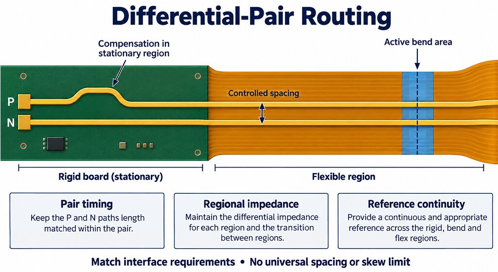
Length compensation also leads to geometry changes. A stationary area is generally preferable for serpentine routing.
Its placement should satisfy both the electrical timing requirement and the mechanical constraints.
8. Via, Pad, and Termination Design
The placement of vias, pads, and terminations should be carefully considered to match their mechanical loading requirements.
Active bend areas should remain clear of connection features wherever practical. Stationary flexible regions may accommodate them when properly supported.
Clearances must identify their measurement references, and the fabricator should confirm compatibility with the proposed construction and tolerances.
8.1. Can You Place Vias in Flexible Regions?
Vias can be used in suitable stationary flexible constructions. Reliability depends on plating, stackup, support, and service conditions.
Active bending can bring the additional risk around the barrel and pads. Layer transitions should therefore remain outside the expected movement envelope wherever possible.
A calculated neutral-axis location does not, by itself, establish via reliability.
8.2. How Far Should Vias Be From the Rigid-Flex Boundary?
Your clearance needs a defined starting point and boundary. Hole-center, hole-wall, and pad-edge measurements produce different values. The rigid edge may also differ from the start of actual bending.
A universal 2 mm limit is not established by the sources used here. Your fabricator should confirm the required value after reviewing the transition construction.
8.3. How Should Pads Connect to Conductors?
The connection should follow the component or termination requirements.
ounded fillets and suitable anchoring features can help support the copper. Coverlay openings determine the exposed area and surrounding restraint.
Pad shape alone cannot establish reliability. An oval pad still needs suitable support and placement outside active bending.
8.4. Where Should Gold Fingers and COB Pads Go?
Gold fingers need controlled contact geometry and insertion thickness. A stiffened flexible tail may meet those requirements.
Chip-on-board (COB) assembly needs support compatible with die attachment, bonding, and encapsulation. PCB assembly provider should review the proposed area.
Both connections need stability during service. Reinforcement boundaries should avoid concentrating movement beside the termination.
9. Grounding, Copper Coverage, and Shielding
The grounding structure must support electrical performance while remaining compatible with bending.
Solid copper, hatched copper, and shielding films affect the finished construction differently.
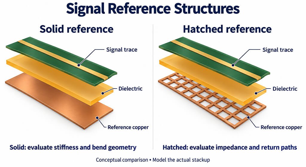
9.1. Choose Between Hatched and Solid Copper
Your reference structure should reflect the actual application.
Structure | Main Benefit | Main Issue To Evaluate |
Solid Copper | Continuous Reference Surface | Added Stiffness And Finished Thickness |
Hatched Copper | Reduced Copper Coverage | Pattern-Dependent Impedance And Return Paths |
Conductive Shielding Film | Additional Shielding Option | Ground Connection And Stackup Compatibility |
A hatch pattern is not automatically equivalent to a solid plane. Its geometry needs appropriate representation in the electrical model.
Likewise, flexible construction does not automatically prohibit solid copper.
9.2. Design the Shielding Structure
Your shield should address an identified interference problem.
The drawing needs to show its extent, material, and ground connection. Shielding performance and signal-reference behavior belongs to design questions.
Film and adhesive additions also change the stackup. Their terminations must remain compatible with the intended bend.
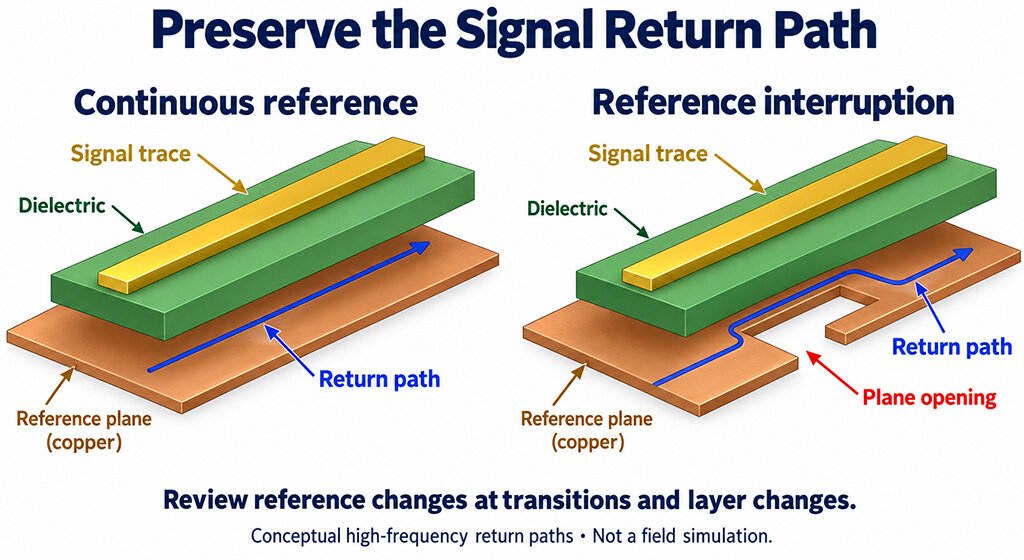
9.3. Preserve Signal Return Paths
The high-speed signal needs a suitable reference throughout the connection.
Texas Instruments recommends continuous ground references and warns against crossing plane splits or voids. Detoured return currents can increase interference and degrade signal integrity.
Where the signal changes reference layers, review the connection between those references.
Analog and digital placement zones do not automatically require split ground planes.
10. Impedance Control and High-Speed Signal Integrity
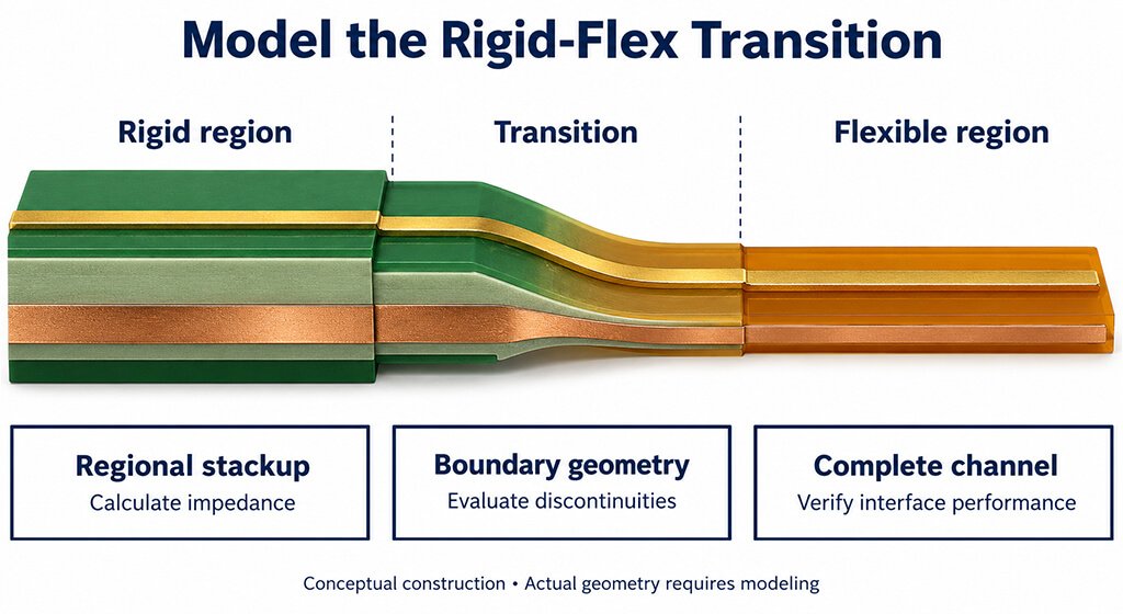
The rigid-flex PCB needs controlled transmission geometry across rigid regions, flexible regions, and their boundaries.
Different dielectrics and reference structures can produce different impedances, even with unchanged trace width.
Regional calculations establish the starting geometry. Demanding interfaces may also need transition analysis and channel measurements representing the installed assembly.
10.1. Model Rigid and Flexible Regions Separately
Characteristic impedance is the voltage-to-current ratio of a traveling wave along a transmission line.
It depends on conductor geometry, dielectric properties, and the reference structure.
Your calculations should include finished copper dimensions, dielectric thicknesses, adhesives, and coverlay.
Material properties need their frequency and test context. Panasonic lists Dk = 3.2 at 1 GHz for R-F775. That value belongs to the specified material; it is not a universal PI constant.
10.2. Control the Rigid-Flex Impedance Transition
The transition needs evaluation beyond the uniform regions.
A width adjustment may help match regional impedances. Its position must also respect bending constraints.
Question | Appropriate evaluation |
Does each uniform section meet its target? | Regional transmission-line calculation |
Does the boundary introduce a significant discontinuity? | Transition modeling |
Does the full connection meet interface requirements? | Channel analysis or measurement |
Connectors, pads, and vias also contribute to the complete channel.
10.3. Maintain Differential-Pair Consistency
The differential pair needs controlled spacing, reference geometry, and timing mismatch.
Equal physical length does not guarantee equal delay when the traces experience different dielectric environments.
TI recommends matching the relevant pair members. Transmit and receive groups do not automatically need equal lengths.
The interface and component requirements should establish acceptable mismatch.
10.4. Evaluate Flexible-Section Loss
The flexible interconnect consumes part of the channel loss budget.
Length, copper properties, dielectric loss, and transitions contribute. Published values need their construction details.
Panasonic reported −2 dB per 100 mm at 6 GHz for a specified three-layer LCP structure. That historical example cannot predict an unrelated stackup.
10.5. Verify Electrical Performance in Relevant Bend States
Your measurements should represent the installed geometry.
Folding may change spacing between conductors, shields, or adjacent sections. Moving applications may require evaluation across several positions.
An impedance coupon represents its own structure. It may not reproduce every board transition.
Your plan should distinguish coupon testing, channel measurement, and interface operation. Each result needs appropriate acceptance limits.
11. How to Verify Rigid-Flex PCB Reliability?
Your verification plan should evaluate the failures expected in the actual application. Electrical tests check connectivity, while impedance measurements characterize selected transmission structures.
Bend testing evaluates defined movement. Assembly and environmental testing address additional loads.
Each method needs acceptance criteria because passing one test does not establish every aspect of reliability.

11.1. Understand Electrical and Impedance Test Coverage
Your test results should remain tied to their scope.
Method | What it establishes | What it cannot establish alone |
Bare-board electrical test | Connectivity and isolation under test conditions | Remaining bend life |
Impedance measurement | Impedance of the measured structure | Complete channel performance |
Application signal test | Operation under tested conditions | Mechanical endurance |
Bend endurance test | Survival under specified movement | Performance in every environment |
Initial electrical measurements provide a baseline for later testing.
11.2. Define the Bend-Life Test
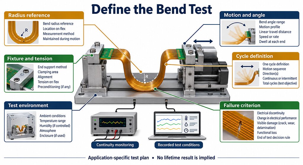
The endurance specification needs motion, fixture, and failure definitions.
It should record the stackup, radius reference, angle, speed, tension, environment, and sample quantity. One cycle must also have an unambiguous meaning.
IPC-TM-650 Method 2.4.3F, May 2022, measures flexes until conductor failure using an etched pattern. It requires at least six specimens, with conductor length oriented in the base material’s transverse direction.
Those requirements belong to that method. Your assembled product may need a separate application test.
11.3. Verify Environmental and Assembly Effects
The qualification should reflect expected temperature, humidity, vibration, and handling.
Installed inspection should confirm where bending actually occurs. Clamps, adhesive, or housing contact can shift it away from the intended location.
The report should preserve construction details, fixtures, sequence, and failure observations. Those records help assess later changes to materials or assembly.
12. How to Diagnose Common Rigid-Flex Failures?
The investigation should begin with the symptom and the conditions that produce it.
Intermittent continuity, cracking, and signal errors can have different causes. Record board position and movement before further testing.
Electrical measurements and targeted inspection can then distinguish conductor damage from a connection, material, or assembly problem.
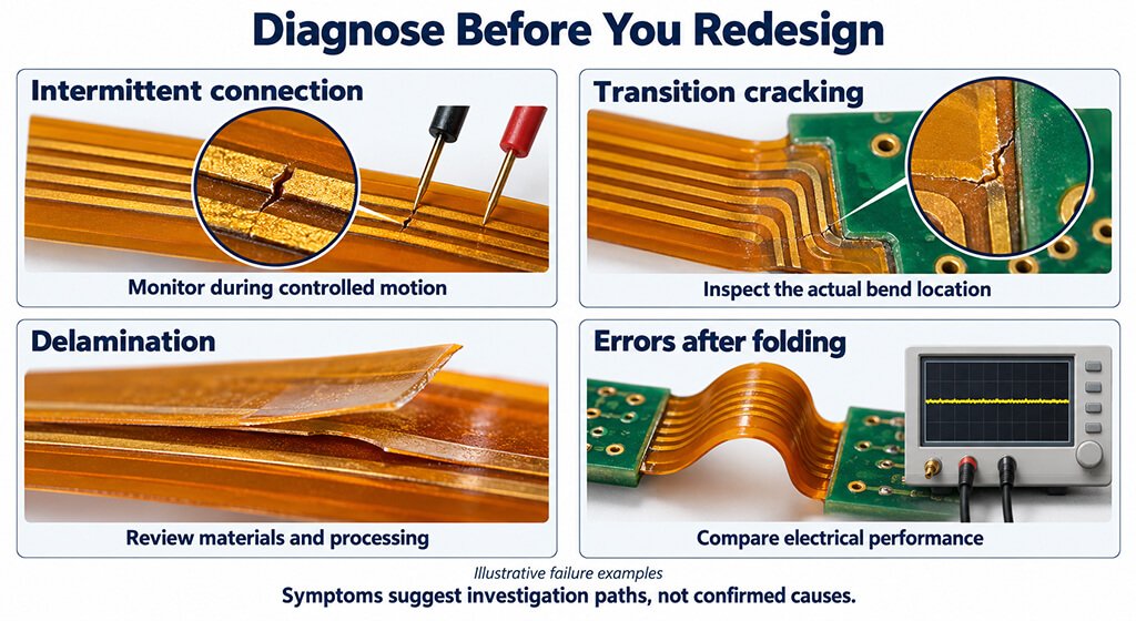
Symptom | Possible Cause | Useful Investigation | Correction To Evaluate |
Continuity Drops During Movement | Conductor or connection damage | Controlled motion with electrical monitoring | Bend geometry or connection support |
Crack Near The Rigid Edge | Concentrated bending or handling damage | Motion inspection and physical analysis | Bend location or assembly procedure |
Pad Lifting | Connection loading or inadequate support | Reinforcement and process inspection | Support coverage or load relief |
Delamination | Bonding, moisture, or thermal effects | Material history and cross-section review | Confirmed process or material issue |
Errors After Folding | Changed coupling or a strained connection | Measurements across controlled positions | Routing, reference structure, or support |
A crack location does not establish the original cause. Assembly may have forced movement into that area.
Your investigation should preserve evidence:
- Record failure conditions and assembly history.
- Compare failed and unfailed samples.
- Narrow the location through electrical measurements.
- Select physical analysis based on the suspected mechanism.
- Test the correction under the conditions that produced failure.
The table provides investigation paths. Confirmed evidence should determine the corrective action.
13. FAQ About Rigid-Flex PCB Design
Can You Use a 10T Radius for Dynamic Bending?
A 10T ratio alone does not establish dynamic reliability.
The radius depends on materials, conductor construction, movement, and required life.
Must Dynamic Traces Be Widened by 20–30%?
No universal percentage applies to every dynamic flexible circuit.
The width must satisfy electrical, manufacturing, and mechanical requirements together. Required transitions should sit outside active bending where practical.
an High-Speed Signals Use Hatched Reference Copper?
Hatched copper may be suitable after evaluating the actual transmission structure.
Your model should account for pattern dimensions, trace position, dielectric spacing, and ground connections.
Channel measurements should confirm compliance with the interface requirements.
14. Conclusion
Your rigid-flex PCB design should connect each layout decision to an operating requirement.
Bending conditions guide materials and stackup, while electrical requirements shape conductor geometry and reference layers.
Fabricator review establishes process suitability. Qualification then evaluates the finished construction under the assembly and service conditions defined for the product.
Before release, your documentation should identify the active bend areas and finished flexible thickness. Radius references, transition clearances, electrical targets, and acceptance criteria also need clear definitions.
If the stackup, mounting arrangement, or motion changes, revisit the affected calculations and tests. The approved drawings and verification records provide the basis for deciding whether the revised design remains suitable.