
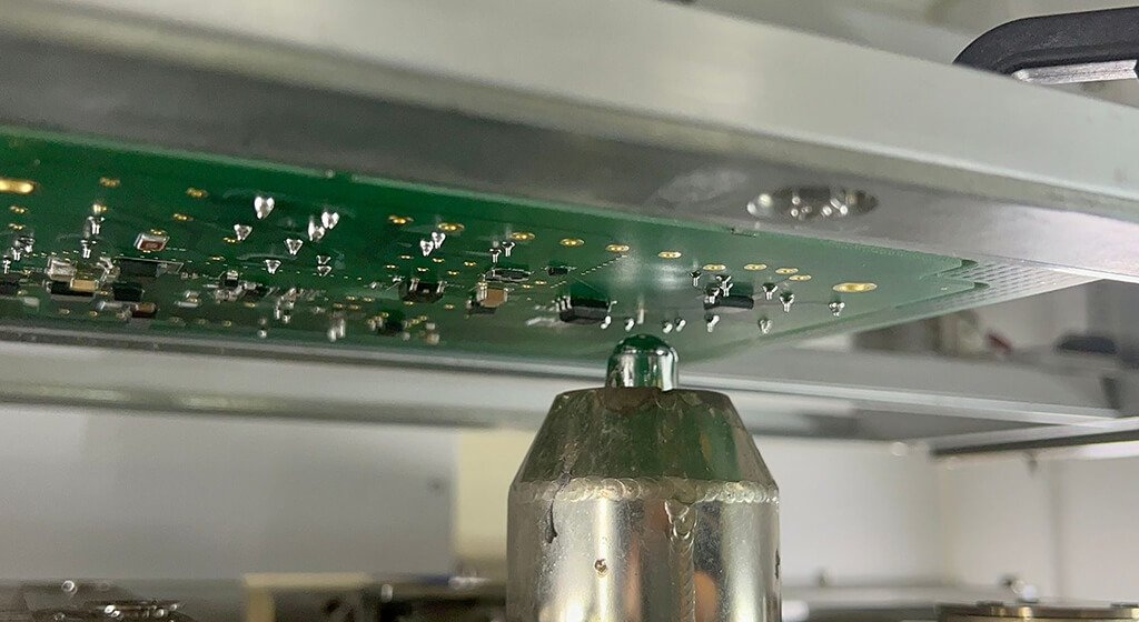
Selective soldering is an automated PCB assembly process that applies flux, heat, and molten solder only to designated through-hole joints.
It is commonly used on mixed-technology PCB assemblies after surface-mount components have completed reflow soldering.
The process can protect nearby bottom-side components from full-wave exposure. However, no single nozzle clearance, preheat temperature, solder-pot temperature, or contact time works for every assembly. These values depend on the PCB, components, materials, equipment, and acceptance requirements.
In the article, we will deep into selective soldering.
Table of Contents
1. What Is Selective Soldering?
Selective soldering is a controlled assembly process that solders chosen through-hole connections without exposing the entire PCB underside to a conventional solder wave.
A typical system applies flux locally, preheats the assembly, and brings a programmable miniature solder wave into contact with defined joints.
The process is especially useful for mixed SMT and through-hole assemblies.
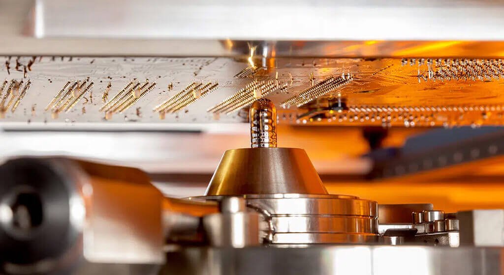
1.1. What Types of PCB Assembly Joints Does It Address?
Selective soldering commonly handles connectors, relays, transformers, terminals, switches, and other through-hole components. These parts may be too large for surface-mount assembly or may require strong mechanical anchoring.
The process is often introduced after Surface Mount Technology (SMT) components have passed through reflow. It allows the manufacturer to solder selected plated through-hole connections while limiting contact with surrounding bottom-side components.
Selective soldering is not automatically the best route for every through-hole joint. A full wave process may be faster when most of the PCB underside can contact solder safely. Pin-in-paste, press-fit, robotic iron soldering, or controlled hand soldering may also be appropriate.
1.2. Is Selective Soldering the Same as Selective Wave Soldering?
The terms are often used interchangeably in PCB assembly. Strictly speaking, selective soldering can describe several localized soldering methods. These include miniature solder waves, selective dip tools, robotic irons, and other targeted processes.
This guide focuses on automated miniature-wave and multi-wave systems. These systems generally follow three main stages: flux application, preheating, and localized molten-solder contact. Ersa’s selective-soldering documentation describes the same sequence and distinguishes mini-wave from multi-wave equipment.
2. How Does the Selective Soldering Process Work?
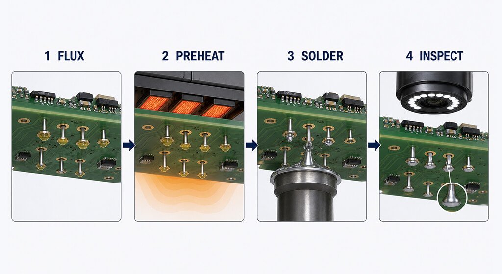
A typical selective soldering process converts PCB design data into a controlled machine program.
The system applies flux to selected locations, preheats the assembly, solders the programmed joints, and records relevant process data. Cooling, cleaning, inspection, and electrical testing may follow.
The exact sequence depends on the machine configuration and product requirements.
Step 1: Targeted Flux Application
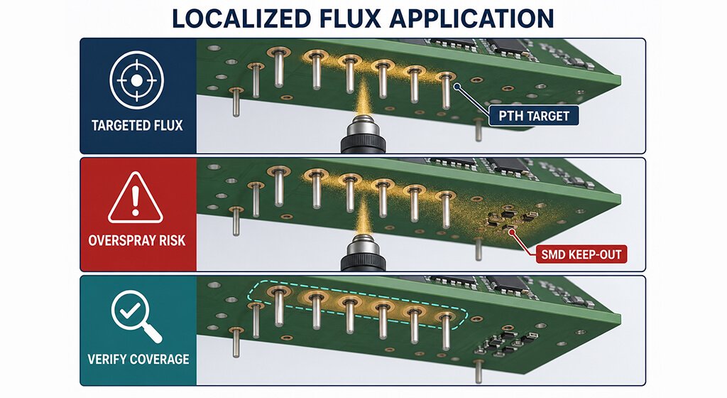
Flux removes surface oxides and supports wetting when molten solder reaches the joint. Selective equipment may use drop-jet, micro-spray, or another controlled application method.
Flux performance depends on more than chemical classification. Its deposited solids, location, spread, activation temperature, and compatibility with the surface finish all matter. Too little flux can contribute to poor wetting or insufficient hole fill. Excess flux can leave residues outside the intended area or create reliability concerns in sensitive products.
Step 2: Preheating the Assembly
Preheating raises the temperature of the PCB, component leads, and plated holes before solder contact. It can reduce thermal shock, activate the flux, and improve heat transfer into high-mass joints.
The correct profile depends on board thickness, copper distribution, laminate, component limits, flux chemistry, and heating method. A machine setpoint alone does not prove that a connector pin or thermally connected barrel reached the intended temperature.
Process engineers should measure the actual assembly response. Thermocouples can be placed near representative high-mass and temperature-sensitive locations. The profile should then be reviewed against material data and component specifications.
Step 3: Localized Soldering with a Mini-Wave or Multi-Wave
A mini-wave system pumps molten solder through a small nozzle. The machine moves the nozzle or PCB so that the solder contacts selected pads and leads.
Controllable variables may include:
- Solder-pot temperature;
- Wave height and stability;
- Nozzle type and diameter;
- Board or nozzle position;
- Immersion depth;
- Contact time;
- Drag speed;
- Approach and exit direction;
- Nitrogen flow, when used.
Single-nozzle systems can apply different settings to individual joints. A multi-wave tool contacts several locations at the same time. The latter may improve throughput, but it requires a product-specific tool.
Step 4: Post-Solder Cooling, Cleaning, and Inspection
After solder contact, the joint cools and the solder solidifies. The required cooling control depends on the alloy, assembly, and equipment.
“No-clean” describes a flux chemistry and qualified residue condition. It does not mean cleaning is unnecessary in every application. High-voltage, high-impedance, humid-environment, conformally coated, or residue-sensitive products may need further evaluation.
Inspection may combine visible-joint review, Automated Optical Inspection (AOI), X-ray imaging, microsection analysis, electrical testing, and functional testing. Each method proves different characteristics.
Process Stage | Controlled Inputs | Expected Result | Useful Production Evidence |
Fluxing | Flux product, deposited amount, position, and spray pattern | Oxides are removed and surfaces are properly activated in the target area | Flux lot, process program, and application verification |
Preheating | Heater settings, heating time, and board loading | Flux is activated and thermal gradients are reduced | Product-specific thermal profile |
Soldering | Solder alloy, nozzle, wave height, temperature, and movement | Adequate wetting and acceptable solder-joint formation | Program version and machine logs |
Cooling | Cooling time and cooling method | Stable and controlled solder solidification | Approved process recipe |
Inspection | Inspection method, sampling plan, and acceptance criteria | Objective evidence that the assembly conforms to requirements | FAI, inspection, test, and deviation records |
3. Selective Soldering Equipment: Mini-Wave and Multi-Wave Systems
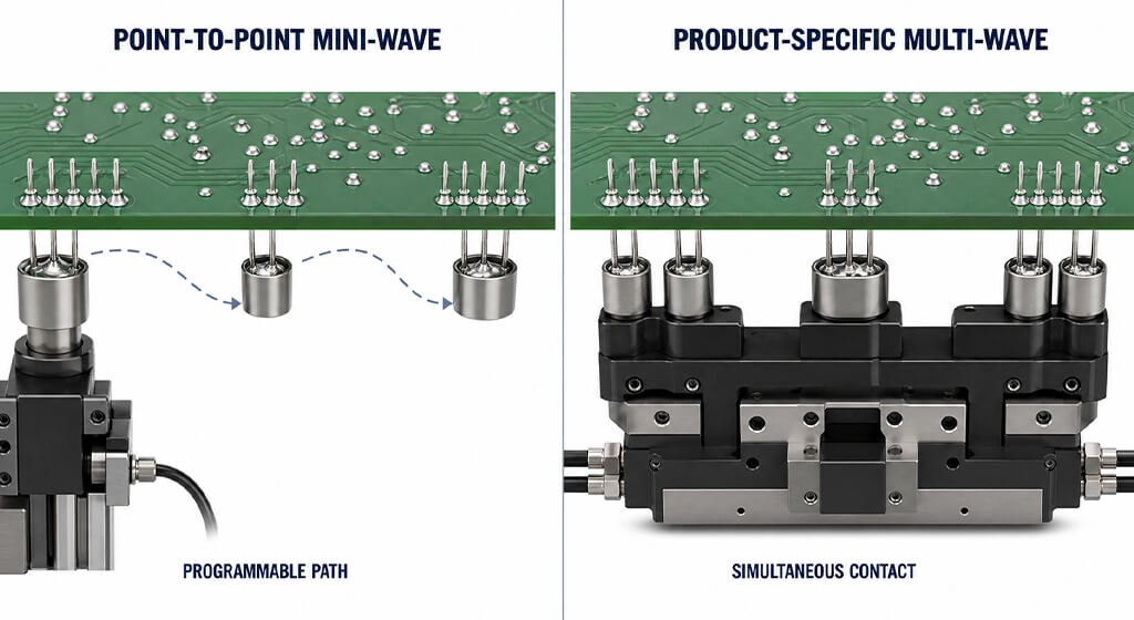
Selective soldering systems generally use a flexible point-to-point mini-wave or a product-specific multi-wave tool. Mini-wave equipment favors programmability and product mix. Multi-wave equipment favors simultaneous soldering and shorter contact cycles.
The right architecture depends on joint count, product stability, volume, allowable tooling cost, and required changeover flexibility.
3.1. Point-to-Point Mini-Wave Soldering
A point-to-point machine uses a single nozzle to solder joints sequentially. It may also drag across a compatible row of pins.
This architecture allows the process engineer to tune contact time, movement, and other settings for different thermal loads. It suits high-mix manufacturing, engineering builds, and products with dissimilar through-hole connections.
The complete cycle time increases as the number of soldering locations grows. Fluxing, preheating, travel, board handling, cooling, and inspection must also be counted.
3.2. Product-Specific Multi-Wave Soldering
A multi-wave system uses a tool with several nozzles positioned for one PCB or panel. Multiple joint groups contact solder at the same time.
This approach can reduce solder-contact time for a stable, high-volume design. It also creates tooling cost and change-control obligations. A layout change can make the existing tool unusable.
Ersa’s selective-system documentation describes both architectures. Its published multi-wave cycle examples are equipment-specific results. They should not be treated as guaranteed line cycle times for an unrelated PCBA.
3.3. Fluxing, Preheating, and Process-Monitoring Options
Equipment configurations vary significantly. Options may include top and bottom preheating, pyrometers, automatic wave-height checks, solder-level monitoring, barcode tracking, and program logging.
4. When Should You Use Selective Soldering?
Selective soldering is a strong candidate when a mixed-technology PCBA has specific through-hole joints but cannot tolerate full-wave exposure. It is also useful when programmable control and repeatability justify more automation than hand soldering.
The final decision should compare design access, production volume, tooling, component limits, inspection needs, and alternative assembly routes.
4.1. Typical Applications and Strong-Fit Conditions
Selective soldering often fits projects with one or more of these conditions:
- Bottom-side SMT components are close to through-hole joints;
- Only a limited portion of the PCB requires through-hole soldering;
- A conventional wave pallet would be difficult or expensive;
- Different joints require different heat inputs;
- Manual soldering would create excessive operator dependence;
- Product traceability requires a controlled machine program;
- Through-hole components are inserted after SMT reflow.
Power electronics, industrial controls, automotive modules, chargers, communication equipment, and medical electronics may use the process. The application category alone does not determine suitability. The actual component layout does.
4.2. Advantages for Mixed-Technology PCBAs
Selective soldering limits flux and solder contact to programmed areas. This can reduce unnecessary thermal exposure and avoid covering the entire PCB underside with flux residues.
A programmable system also supports joint-specific control and repeatable motion. Process data may be easier to retain than with uncontrolled manual soldering.
These advantages improve process capability only when the design and program are suitable. Selective soldering does not eliminate bridging, insufficient hole fill, solder balls, residue risks, or thermal damage.
4.3. Limitations and Cost Tradeoffs
Nozzle access is a primary limitation. Nearby components, board edges, carriers, tall housings, and underside hardware may block the required path.
High-copper or thick PCBs can still be difficult to heat. A small nozzle may provide less energy than the joint requires. Extending contact time without validation can damage the board, connector, or plating.
Programming, fixtures, profiles, first articles, and product-specific tooling create nonrecurring engineering costs. These costs can be economical over repeat production but excessive for a very small build.
4.4. A Practical Go/No-Go Checklist
Before choosing the process, ask:
- Which joints require through-hole soldering?
- Are bottom-side SMT components inside the potential wave-exposure area?
- Can a mini-wave nozzle reach every target without collision?
- Is a wave-solder pallet feasible?
- Are the component heat limits documented?
- Does the expected volume support programming and tooling costs?
- Which joints, if any, will remain manual?
- What inspection evidence is required?
- Could pin-in-paste or press-fit remove a secondary soldering operation?
A “yes” to selective soldering should result from this review, not from the presence of a selective machine at the factory.
5. Choosing Among Selective Soldering and Other Through-Hole Assembly Routes
Selective soldering offers localized automation, but it is one of several through-hole assembly routes. Wave soldering often wins on volume when the underside is accessible. Hand soldering can suit low quantities or exceptions. Pin-in-paste combines through-hole and reflow assembly, while press-fit avoids solder. Design compatibility and total process risk should drive the choice.
5.1. Where Wave Soldering Fits
Wave soldering exposes a broad area of the PCB underside to flux and a solder wave. It can process many through-hole joints quickly, especially when the underside is open or a suitable pallet protects other features.
Selective soldering reaches only defined areas. This supports mixed-technology layouts but usually requires more programming and travel time.
5.2. Where Hand or Robotic Iron Soldering Fits
Hand soldering is flexible and has low initial tooling cost. Its results can depend on operator access, technique, tip condition, feeding, and time at each joint.
Robotic iron soldering reduces some variation but still requires suitable tip access and wire-feed control. A miniature solder wave transfers heat differently and can solder several leads during one movement.
Manual processing may remain appropriate for inaccessible or very low-volume joints. Those exceptions should be listed on the assembly drawing and included in the inspection plan.
5.3. Where Pin-in-Paste and Press-Fit Fit
Pin-in-paste, also called intrusive reflow, prints solder paste into or around plated holes. Through-hole components are inserted before reflow and soldered during the SMT thermal cycle. The component must tolerate the reflow profile, and the paste volume must support the required joint.
Press-fit uses compliant pins inserted into controlled plated holes. It avoids a soldering operation but requires a compatible connector, hole construction, press setup, and force monitoring.
Assembly Method | Strongest Fit | Bottom-Side Exposure | Main Setup Need | Principal Limitation |
Selective Soldering | Mixed SMT/THT assemblies with localized THT joints | Limited to programmed areas | Program, fixture, and nozzle validation | Nozzle access and sequential cycle time |
Wave Soldering | High-volume THT assemblies with accessible underside | Broad wave exposure | Pallet when protection or masking is required | Bottom-side interference |
Hand Soldering | Low-volume production, prototypes, or documented exceptions | Local soldering-iron contact | Work instruction and trained operator | Operator dependence and limited throughput |
Robotic Iron Soldering | Repeatable, accessible solder joints | Localized tip contact | Tip path and wire-feed program | Tip access and equipment maintenance |
Pin-in-Paste | Reflow-compatible THT components | Reflow heats the full assembly | Stencil and solder-paste volume design | Component temperature limits and paste volume |
Press-Fit | Compatible compliant-pin connector systems | No solder exposure | Controlled hole dimensions and press process | Component and hole compatibility |
5.4. Process-Selection Decision Table
Use this table to select a starting route before product-specific DFM and validation.
Assembly Condition | Preferred Starting Route | Why | What Must Be Validated |
Most underside THT joints are accessible and heat tolerant | Wave Soldering | Usually provides better throughput for broad joint coverage | Pallet design, masking, shadowing, and thermal exposure |
Only selected THT joints require soldering near bottom-side SMT parts | Selective Soldering | Limits flux and molten solder exposure to programmed locations | Nozzle access, keep-out geometry, preheat, contact time, and first-article results |
THT components tolerate reflow and adequate paste can be printed | Pin-in-Paste | May eliminate a separate soldering operation | Paste volume, component coplanarity, hole fill, and reflow limits |
Connector and plated holes are designed for compliant pins | Press-Fit | Eliminates the soldering step | Finished-hole dimensions, plating integrity, insertion force, and connector requirements |
Volume is very low or the joint is an isolated exception | Controlled Hand or Robotic Soldering | Avoids dedicated selective tooling for a small number of joints | Work instructions, operator qualification, temperature control, and inspection evidence |
6. Selective Soldering DFM: What Must Be Checked Before Release?
Selective soldering Design for Manufacturability (DFM) must confirm nozzle access, component clearance, hole and lead compatibility, heat flow, board support, and surface solderability.
These conditions depend on the selected equipment and assembly. A fixed internet keep-out value cannot replace a three-dimensional review using the actual nozzle, fixture, PCB tolerances, and component bodies.
6.1. Identify Machine-Soldered, Protected, and Manual Joints
The assembly drawing should identify which joints are machine-selective, wave-soldered, press-fit, or manually soldered. It should also show no-solder areas and components requiring special protection.
This mapping prevents hidden process changes during production. It also allows the customer to approve any manual exception before release.
6.2. Verify Nozzle Access and Component Keep-Out
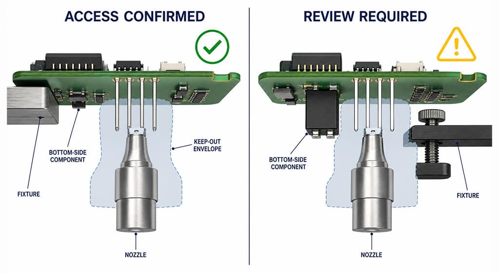
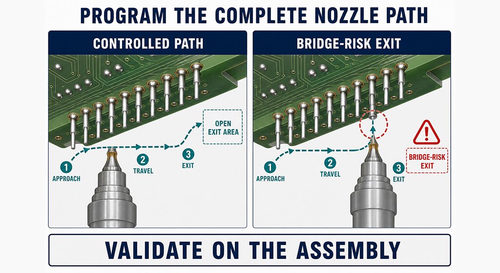
The nozzle must approach, contact, move, and exit without striking adjacent parts. Access depends on more than the nearest pad-to-component distance.
The review should consider:
- Nozzle outside diameter and wettable surface;
- Component body height;
- Pin length;
- Board-edge clearance;
- Fixture and support geometry;
- Board warp;
- Machine positioning tolerance;
- Solder-wave behavior;
- Travel and exit direction.
A universal 3 mm, 5 mm, or 8 mm clearance is not technically defensible. Equipment families and nozzle designs differ. The supplier should confirm the layout using its actual configuration.
6.3. Design the Lead-to-Hole, Pad, and Annular-Ring System
The finished hole must accept the lead across manufacturing tolerances while leaving space for flux, gas escape, and solder flow. Round, rectangular, and irregular leads require different calculations.
DFM should compare the maximum lead envelope with the finished-hole range. The analysis must include plating, drill tolerance, component tolerance, and insertion needs.
Pad and annular-ring design also affects heat transfer and manufacturability. The customer drawing, applicable PCB standard, electrical requirements, and fabricator capability should control the final geometry.
6.4. Manage Copper Planes and High-Thermal-Mass Connections
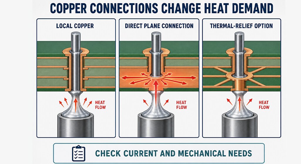
Heavy copper, large planes, thick boards, and high-current connectors can draw heat away from the plated hole. This may prevent solder from reaching the destination side before another part reaches its temperature limit.
Thermal relief can reduce heat sinking, but it is not mandatory for every design. High-current, mechanical, or thermal requirements may justify a solid connection. The correct decision balances electrical performance against solderability.
An IPC-hosted technical paper on selective-soldering design examines hole fill, nozzle selection, spacing, thermal mass, and movement. Its findings support evaluating these factors together rather than treating one variable as the sole cause.
6.5. Account for Tall Components, Board Edges, Fixtures, and Warpage
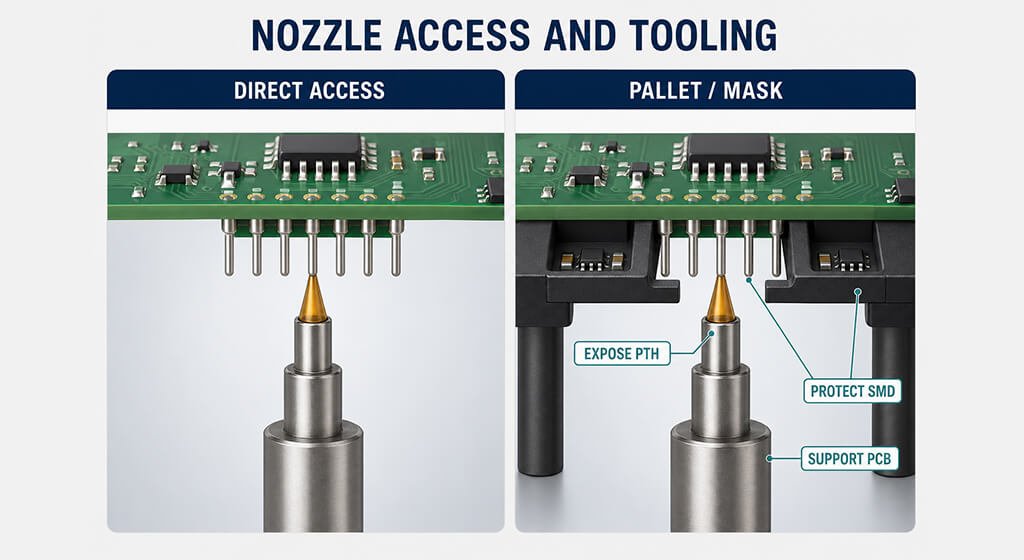
A two-dimensional clearance check can miss real collisions. Connector overhang, leads, heat sinks, bottom-side capacitors, carriers, and clamps may enter the machine envelope.
Board support is equally important. Warpage changes nozzle-to-board distance and immersion depth. The fixture must locate the PCB consistently without covering target areas or damaging components.
6.6. Confirm Surface Finish and Incoming Solderability
Surface finish preserves solderability during storage and assembly. However, previous thermal cycles, handling, contamination, and aging can change the result.
Organic Solderability Preservative (OSP) may already have experienced an SMT reflow cycle before selective soldering.
When solderability is uncertain, IPC J-STD-003D covers printed-board solderability tests. EIA/IPC/JEDEC J-STD-002E addresses component leads and terminations.
Design Feature | Potential Failure | Evidence Needed | Possible Engineering Action |
Tight Bottom-Side Spacing | Nozzle collision or unintended solder wetting | 3D clearance review using the actual nozzle | Move the component, change the nozzle, or select another soldering process |
Heavy Copper Connection | Insufficient solder fill due to high thermal demand | Thermal profile and first-article results | Adjust the heat path, preheat, nozzle, or PCB layout |
Small Finished-Hole Clearance | Poor insertion or restricted solder flow | Lead and finished-hole tolerance analysis | Revise the finished-hole size or component selection |
Large Hole Clearance | Weak joint geometry or excessive solder drainage | Drawing review and first-article inspection | Adjust hole size, pad geometry, or lead selection |
Aged or Reflowed Surface Finish | Nonwetting or dewetting | Incoming solderability evidence | Improve storage conditions, surface finish, flux selection, or incoming controls |
Flexible or Warped Panel | Variable immersion depth and inconsistent joint quality | Warpage measurement and fixture evaluation | Add mechanical support or revise panelization |
7. How Is a Selective Soldering Process Window Established?
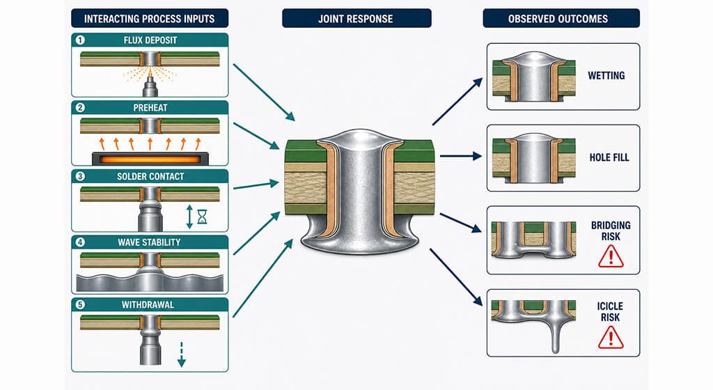
A selective soldering process window is established by connecting controllable inputs to measurable assembly results.
Engineers start with material and equipment recommendations, then profile and inspect the actual PCBA. Approved limits should cover normal variation without exceeding component or board constraints.
The final recipe belongs to the product, machine configuration, alloy, flux, nozzle, and fixture combination.
7.1. Flux Selection, Deposition, and Activation
Flux selection begins with the required activity, residue behavior, alloy compatibility, surface finish, application method, and reliability environment. Its classification alone does not define the production recipe.
A product Technical Data Sheet (TDS) may provide a starting range. Kester’s SELECT-10 selective flux data, for example, is specific to that formulation. Its guidance should not be applied automatically to a different flux.
The process should confirm that the flux reaches the required area, remains active until solder contact, and does not create unacceptable residue elsewhere.
7.2. Preheat Profile and Board Temperature
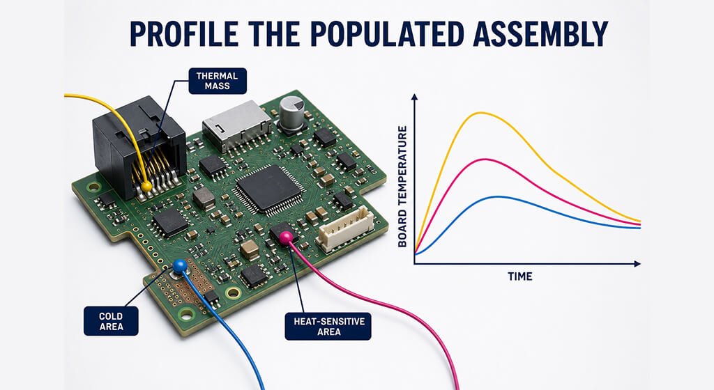
The profile must measure the populated board, not just heater air or machine power. Thermocouples should represent high-mass joints, sensitive components, and relevant board areas.
The selected locations depend on the product. A single board-center measurement may miss the coldest barrel or hottest connector housing.
IPC-7530B addresses temperature profiling for mass soldering equipment, including selective soldering systems. Its product-specific profiling principles are useful, but it does not provide one universal selective-soldering recipe.
7.3. Solder Alloy, Pot Temperature, and Atmosphere
The alloy’s melting range is a material property. The required solder-pot setting is a process choice.
For example, supplier data lists SAC305 with a solidus near 217°C and a liquidus near 220°C. That does not mean the solder pot should operate at 220°C. Heat transfer, dwell time, nozzle behavior, flux, board mass, and component limits affect the working setting.
Nitrogen may reduce oxidation and dross or support wetting in some processes. It can also change solder behavior. The need and oxygen target should be validated rather than described as mandatory.
7.4. Contact Time, Immersion Depth, Wave Height, and Exit Direction
These variables interact. Increasing contact time may improve heat transfer but increase thermal exposure and copper dissolution. Raising wave height may improve contact but also increase bridging or unintended wetting.
Exit direction and speed affect solder separation from the leads. A program that works for one connector orientation may not produce the same result after a layout rotation.
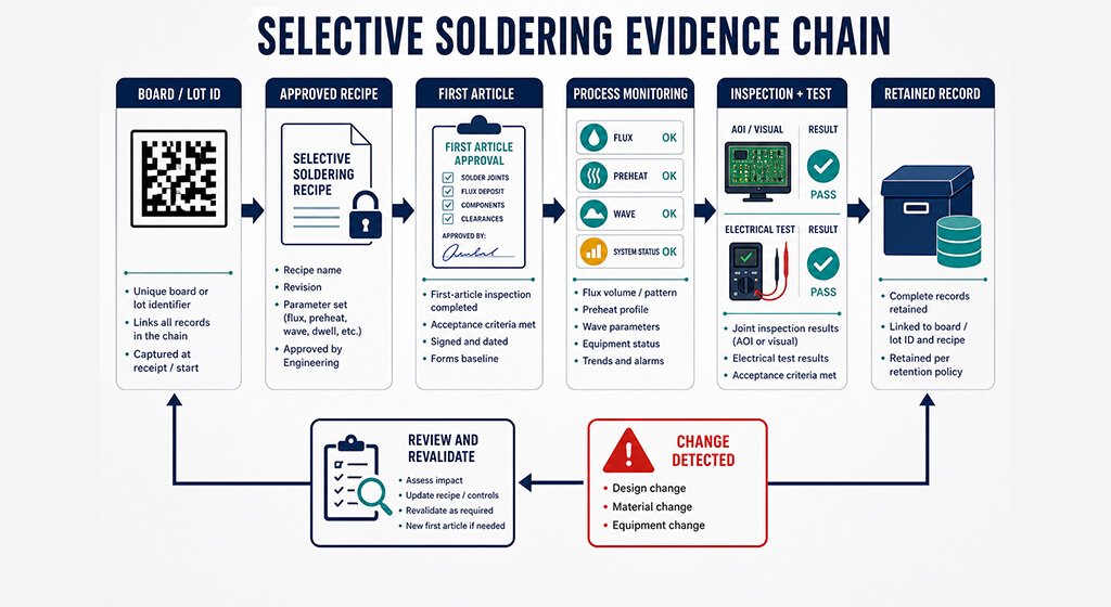
Engineers should change one or a controlled group of variables, record the response, and retain the approved result.
7.5. Product-Specific Validation with First Articles or DOE
A robust setup usually follows this sequence:
- Identify high-risk joints and component limits.
- Establish starting settings from approved material and equipment data.
- Attach thermocouples at representative locations.
- Run first articles.
- Inspect visible and hidden characteristics using suitable methods.
- Adjust the process through controlled trials or Design of Experiments (DOE).
- Freeze the approved program, fixture, nozzle, alloy, and flux.
- Define changes that require review or revalidation.
The following source examples illustrate why values must retain their original context.
|
Published Value |
Source Category |
Correct Interpretation |
|
SAC305 melts across approximately 217–220°C |
Alloy property, not a universal solder-pot temperature or process setting |
|
|
Product guidance for SELECT-10 |
Starting guidance for one selective-solder flux formulation; use the current TDS for exact process parameters. Kester identifies SELECT-10 as a zero-halogen, no-clean liquid flux designed for selective soldering. (Kester) |
|
|
Tg, decomposition temperature, T288, and CTE for R-1755M |
Properties of one specific laminate system, not representative of all FR-4 materials. Panasonic lists, for example, Tg values of 150–175°C depending on test method and Td of 355°C. (industrial.panasonic.com) |
|
|
260°C maximum for 5 seconds during wave soldering for the specified SGI 2.0 header family |
A component-family-specific soldering limit. TE specifies 260°C for a maximum of 5 seconds for wave soldering; this should not be assigned to unrelated connectors. (te.com) |
8. Common Selective Soldering Defects and Root Causes
Common selective soldering defects include insufficient hole fill, bridges, icicles, solder balls, nonwetting, thermal damage, and harmful residues.
A symptom rarely proves one cause. Troubleshooting should connect the defect to physical evidence, then separate design, material, equipment, and process contributions. Changing temperature or contact time without this analysis can hide one defect while creating another.
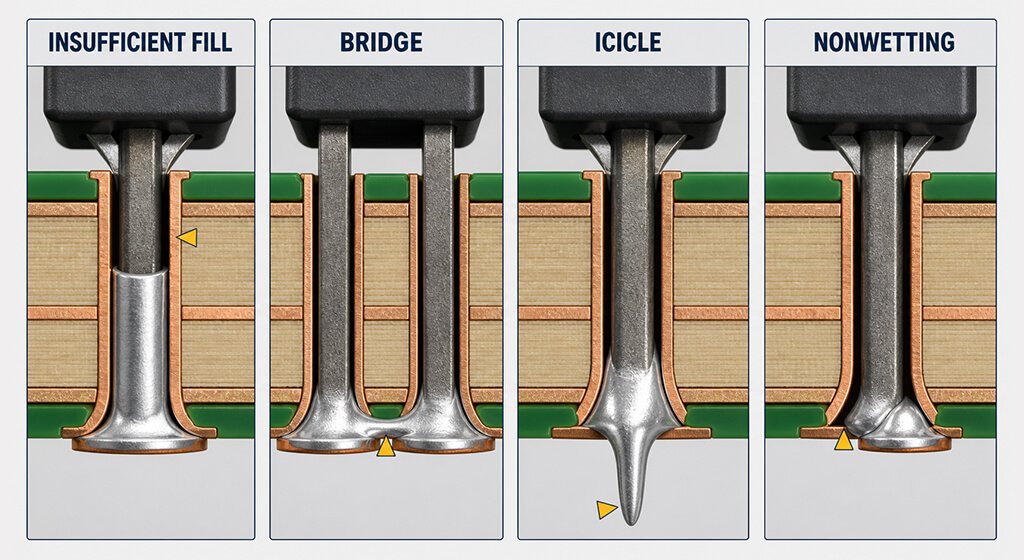
8.1. Insufficient Through-Hole Fill
Insufficient fill can result from inadequate heat transfer, poor solderability, restricted capillary flow, incorrect flux application, or an unsuitable hole-to-lead relationship.
Start by comparing cold and normal joints. Check their copper connections, component finish, flux pattern, and profile. If only plane-connected pins fail, thermal mass deserves attention. If pins across several thermal conditions fail, incoming solderability or flux application may be more likely.
8.2. Bridges, Icicles, and Excess Solder
Bridges form when solder remains between conductors that should be isolated. Exit direction, lead length, spacing, wave dynamics, alloy contamination, flux, and atmosphere can influence separation.
Icicles often indicate that solder did not release cleanly. Increasing speed may help in one geometry and worsen another. Video, joint orientation, and machine data can reveal more than a visual defect list alone.
8.3. Solder Balls and Spatter
Solder balls may originate from solder-mask interaction, moisture, flux behavior, preheat, oxide films, or mechanical splashing. Their location provides useful evidence.
Balls clustered along a movement path suggest a different mechanism from balls distributed across the board. Inspection should document size, location, frequency, and relationship to the selective path.
8.4. Nonwetting, Dewetting, and Incomplete Fillets
Nonwetting occurs when solder does not establish the intended metallurgical bond. Dewetting occurs when solder initially wets and then withdraws, leaving irregular coverage.
Possible causes include oxidized finishes, contamination, inadequate flux activity, excessive delay after fluxing, or an unsuitable thermal condition. Incoming PCB and component solderability should be investigated before repeatedly increasing machine heat.
8.5. Thermal Damage, Warpage, Pad Lifting, or Barrel Damage
Excessive or repeated heat can damage connector housings, laminate, pads, plating, solder mask, and adjacent parts. Cumulative exposure matters when a PCBA has already completed reflow or rework.
The investigation should compare actual temperature-time data with the exact component and material limits. “Lead-free compatible” does not define every permissible process cycle.
8.6. Flux Residue and Electrochemical Reliability Risks
Residue risk depends on chemistry, location, activation, electric field, humidity, spacing, and product environment. A visually clean board may still contain harmful ionic material, while visible benign residue may be acceptable under a qualified process.
ISO 9455-17:2024 provides a method for evaluating Surface Insulation Resistance (SIR) and electrochemical migration effects from flux residues. Production acceptance must still reflect the product and customer requirements.
Defect | Likely Causes | Prevention and Process Control |
Insufficient Barrel Fill | Weak flux activity, inadequate preheat, short contact time, poor solderability, high thermal mass, or unfavorable lead-to-hole geometry | Confirm solderability, balance thermal mass, validate flux deposition, and establish a measured preheat and contact-time window |
Solder Bridging | Excessive solder contact, unfavorable withdrawal, closely spaced pins, poor drainage, oxide buildup, or unstable solder flow | Optimize nozzle selection, path, withdrawal direction, contact time, solder condition, and localized nitrogen use where justified |
Icicles or Excessive Solder | Slow drainage, low board or lead temperature, poor withdrawal settings, excessive solder pickup, or disturbed flow | Adjust preheat, withdrawal speed, nozzle path, contact time, and drainage orientation |
Solder Balls or Spatter | Excess flux, incomplete solvent evaporation, moisture, aggressive immersion, contaminated fixtures, or incorrect preheat | Control flux quantity and spray pattern, verify evaporation, manage moisture, and maintain fixtures |
Nonwetting or Dewetting | Oxidized leads or pads, contamination, insufficient flux activity, or incompatible surface condition | Protect storage conditions, verify component and PCB solderability, confirm flux compatibility, and control handling |
PCB Warpage or Thermal Damage | Excessive temperature, prolonged heat exposure, inadequate support, high thermal gradients, or component-limit violations | Use adequate support, validate full thermal history, respect component limits, and reduce unnecessary dwell |
Flux Residue or Electrochemical Risk | Excessive deposit, incomplete activation, incompatible cleaning, or residue trapped under low-standoff components | Use a validated flux process, control deposition, follow supplier cleaning guidance, and define project-specific cleanliness acceptance |
9. How Should Selective Solder Joints Be Inspected and Validated?
Selective solder joints should be validated through methods matched to the characteristic being assessed.
Visual inspection and AOI evaluate visible conditions. X-ray may support analysis of concealed solder distribution. Microsection reveals internal structure destructively. Electrical and functional tests confirm circuit behavior.
No single method proves every workmanship, internal-fill, reliability, and functional requirement.
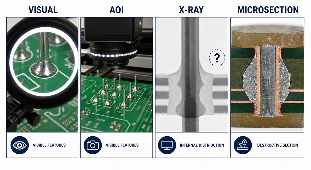
9.1. Visual Inspection and AOI: What They Can See
Visual inspection and AOI can detect visible bridges, solder balls, incomplete external fillets, component presence, polarity, and other accessible conditions.
AOI cannot see through an opaque PCB or connector body. It should not be presented as proof of complete internal barrel fill.
9.2. X-Ray Inspection: When It Helps
X-ray imaging can reveal solder distribution that is not visible optically. Its usefulness depends on joint geometry, viewing angle, resolution, component overlap, and analysis technique.
A standard two-dimensional image may not provide an unambiguous fill measurement for every through-hole joint. The inspection plan should define what the image must show and how the result will be interpreted.
9.3. Microsection: Destructive Process Validation
Microsection analysis cuts and prepares a representative joint so that internal fill, plating, interfaces, and defects can be examined.
Because the sample is destroyed, microsection is usually applied during process development, qualification, first-article validation, or failure analysis. Sampling and location should target meaningful risk rather than a convenient joint.
9.4. Electrical and Functional Testing: What They Do Not Replace
In-Circuit Test (ICT), continuity testing, and Functional Circuit Test (FCT) can detect opens, shorts, incorrect components, and functional failures.
A joint can pass an electrical test while still having workmanship or long-term reliability concerns. Electrical testing therefore complements rather than replaces appropriate solder-joint inspection.
10. Which Standards Apply to Selective Soldering?
Selective soldering is governed through several standards rather than one universal process specification.
IPC J-STD-001 addresses soldering process and material requirements, while IPC-A-610 addresses post-assembly acceptability.
Other documents cover solderability, flux, alloys, components, rework, residues, materials, laboratories, and measurement traceability. The customer contract determines which documents and revisions apply.
10.1. J-STD-001 and IPC-A-610: Process Requirements vs. Acceptance
IPC J-STD-001J and IPC-A-610J were released in 2024. IPC describes J-STD-001 as the industry-consensus standard for soldering processes and materials. IPC-A-610 is the post-assembly acceptability standard.
These documents are often used together, but they serve different roles. A supplier should identify the contracted revision, product class, amendments, and customer exceptions.
Neither document means that a Class 3 assembly must use selective soldering. The assembly route is a manufacturing decision unless the contract states otherwise.
10.2. J-STD-002, J-STD-003, J-STD-004, and J-STD-006
These standards address supporting parts of the process:
- J-STD-002: component lead and termination solderability;
- J-STD-003: printed-board solderability;
- J-STD-004: soldering-flux requirements and classification;
- J-STD-006: electronic-grade solder alloys and solid solder products.
The current revision should be checked in the IPC document revision table before publication or contract release
10.3. JEDEC and Component Datasheets
IPC/JEDEC J-STD-020 classifies moisture/reflow sensitivity for applicable nonhermetic SMDs. It does not provide a universal selective-soldering contact limit.
EIA/IPC/JEDEC J-STD-075 addresses process sensitivity for non-IC components. The standard explains that industry worst-case limits are not recommended assembly parameters. The exact component supplier remains the primary source for a part’s soldering and handling limits.
10.4. ISO, UL, and NIST
ISO 9001 establishes Quality Management System requirements. Certification indicates a controlled management system, not automatic compliance of each solder joint with IPC criteria.
ISO/IEC 17025:2017addresses testing and calibration laboratory competence. Accreditation applies to the laboratory’s stated scope.
UL 796 and UL 796F assembly-solder revisions treat assembly soldering limits as critical PWB recognition parameters. A UL Recognized board material or construction is not the same as a UL Listed end product.
NIST’s metrological traceability policy requires a documented, unbroken calibration chain for a traceable measurement result. NIST also explains that traceability alone does not guarantee fitness for purpose. The measurement uncertainty must be suitable for the decision.
Source | Primary Role | Does Not Establish |
IPC J-STD-001 | Soldered-assembly process and material requirements | Mandatory use of selective soldering |
IPC-A-610 | Post-assembly acceptability criteria | A complete production process |
J-STD-002 / J-STD-003 | Component and PCB solderability testing | Product-specific machine settings |
J-STD-004 / J-STD-006 | Flux and solder material requirements | One universal process window for all materials |
J-STD-020 / J-STD-075 | Component sensitivity and handling classification | Universal PCBA temperature settings |
ISO 9001 | Quality management system requirements | Joint-level acceptance criteria |
ISO/IEC 17025 | Laboratory competence and testing capability | Accreditation beyond the stated scope |
UL 796 / UL 796F | Recognized PWB constructions and applicable solder-related limits | Certification of the complete end product |
NIST Policy | Measurement traceability and metrology principles | Process capability or product acceptance criteria |
11. What Determines Selective Soldering Cost and Cycle Time?
Selective soldering cost and cycle time depend on the complete manufacturing route, not solder contact alone. Joint count, fluxing, preheating, nozzle travel, panelization, handling, cooling, inspection, tooling, and product changeovers all contribute.
A multi-wave tool can shorten soldering time, but its economics depend on volume, design stability, maintenance, and expected product life.
11.1. Cycle-Time Drivers
A supplier should calculate:
- Load and unload time;
- Barcode or product verification;
- Fluxing movement;
- Preheat and stabilization;
- Soldering path;
- Nozzle cleaning or conditioning;
- Cooling;
- Inspection and testing;
- Panel separation, when applicable.
Two PCBAs with the same number of through-hole pins can have very different cycle times. Joint grouping, thermal mass, and travel distance matter.
11.2. Tooling, Programming, and NRE
Nonrecurring engineering may include DFM, fixture design, nozzle selection, programming, profiling, first articles, inspection programming, and destructive validation.
These costs should be separated from recurring unit cost. Clear separation helps an OEM compare a small pilot build with repeat production.
11.3. When Can Multi-Wave Tooling Be Economical?
Multi-wave tooling becomes more attractive when the design is stable, the same joints repeat across substantial volume, and cycle-time savings exceed tooling and maintenance costs.
A point-to-point system may remain better for frequent variants. The correct comparison uses expected annual quantity and change frequency, not only the fastest published machine cycle.
12. FAQ About Selective Soldering
When Should Engineers Prefer Selective Soldering?
Engineers should prefer selective soldering when only defined through-hole areas can contact solder or when bottom-side SMT components prevent full-wave exposure. Wave soldering may be faster and less expensive when many joints are accessible. The decision should include tooling, cycle time, DFM, thermal risk, inspection, and expected production volume.
Can Selective Soldering Be Used for High-Volume Production?
Yes. High-volume production can use multi-nozzle tools, parallel processing, dual pots, or multiple machines. However, high volume does not automatically justify selective soldering. A wave process may have lower cycle time when the design permits it. The economic decision should use complete line throughput, tooling cost, change frequency, and yield.
Does Selective Soldering Require Nitrogen?
No universal standard requires nitrogen for every selective soldering process. Nitrogen may reduce oxidation, dross, or wetting variation in a qualified setup. Its benefit depends on alloy, flux, equipment, surface condition, and joint geometry. The supplier should validate the oxygen level and resulting joint quality instead of treating nitrogen as a marketing checkbox.
What Temperature Is Used for Selective Soldering?
There is no universal selective soldering temperature. The alloy melting range, flux activation window, PCB thermal mass, component limits, nozzle, and contact time all affect the setting. Supplier TDS values can establish a starting point, but engineers should measure the actual assembly profile and validate the joints before approving production.
Can It Be Used on Boards with Bottom-Side SMT Components?
Yes. Protecting bottom-side SMT components is one of the main reasons to choose selective soldering. Those components must still remain outside the nozzle, solder wave, flux pattern, and thermal-risk envelope. DFM should consider component height and body shape, not only pad-to-pad distance.
What Causes Insufficient Through-Hole Fill?
Common causes include inadequate heat transfer, high copper mass, poor PCB or lead solderability, insufficient flux, unsuitable hole-to-lead clearance, and short solder contact. Troubleshooting should compare the affected joints with thermal connections, material lots, profile data, and flux records before changing the process.
13. Final Takeaway: Treat Selective Soldering as a Controlled Process Decision
Selective soldering is valuable when a mixed-technology PCBA requires localized through-hole soldering and controlled exposure. Its success depends on more than machine ownership.
The design must provide access, the materials must remain solderable, and the process window must be validated on the actual assembly.