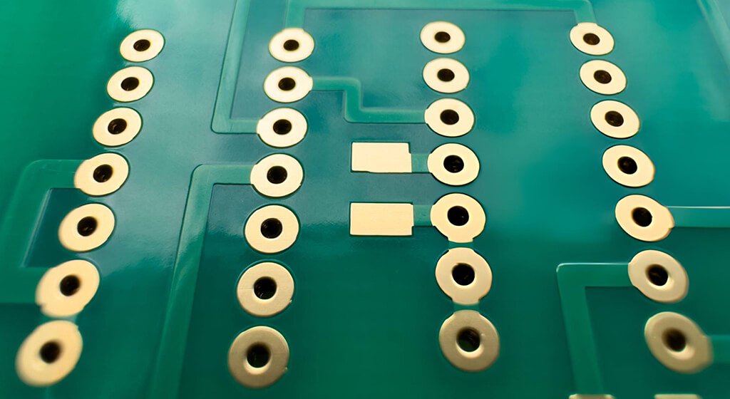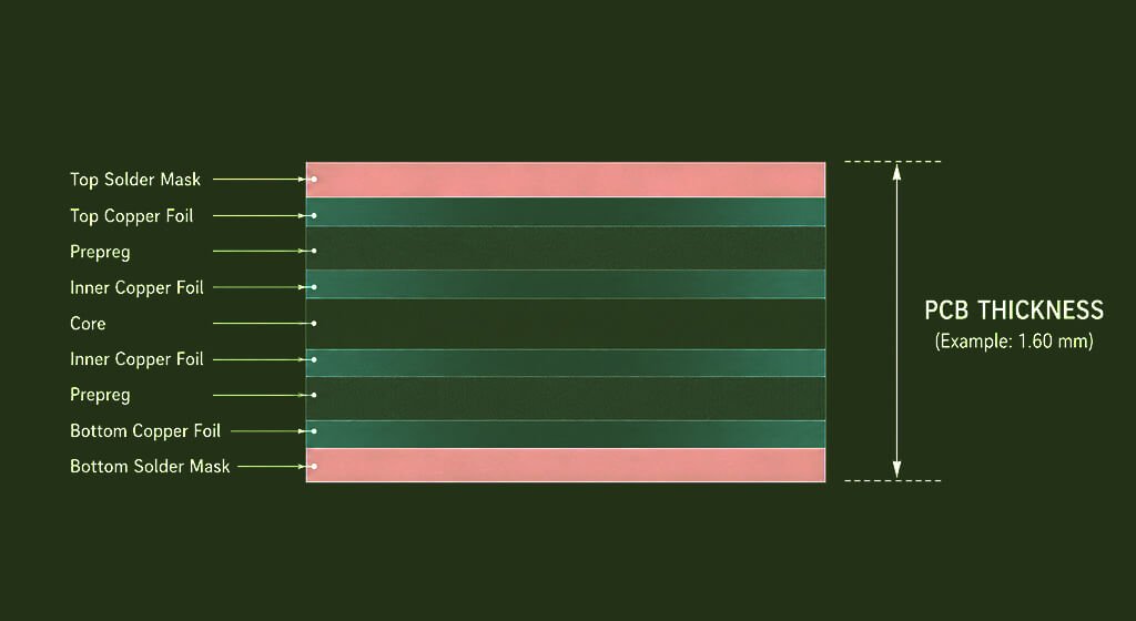
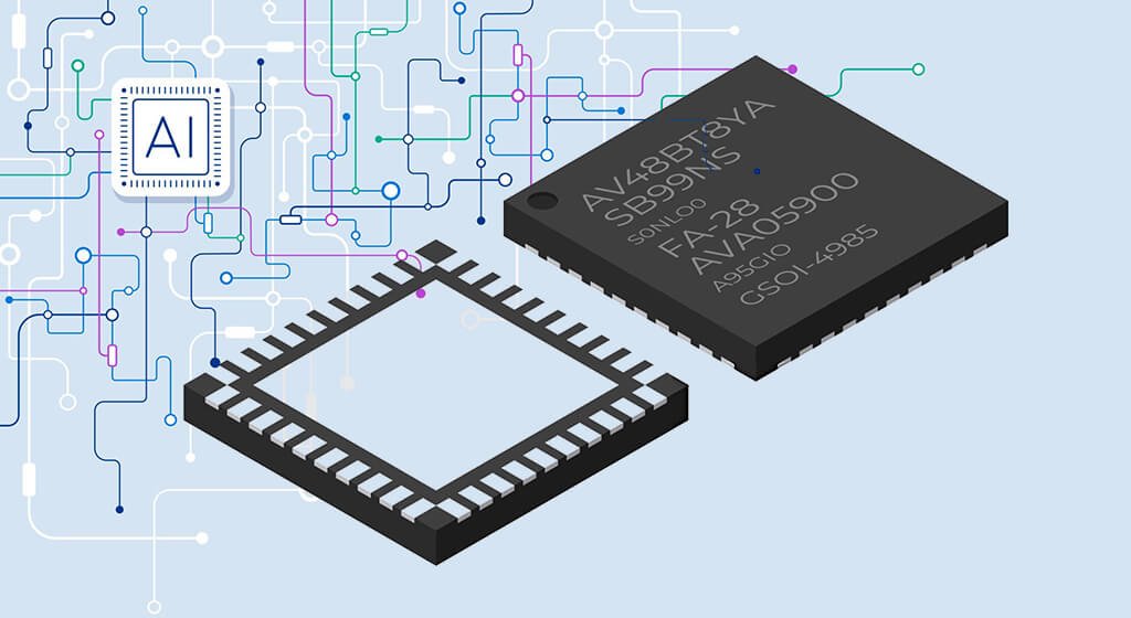
A QFN package, or quad flat no-lead package, is a low-profile surface-mount IC package with flat electrical terminals around its underside perimeter.
Many QFNs also have a large exposed pad beneath the body for heat transfer and, when specified, electrical grounding.
QFNs save board space and shorten interconnections, but their hidden solder joints demand careful PCB design, paste printing, reflow, and inspection.
In this article, we will deep into QFN Package’s Design, Assembly, and Inspection and so on.
Table of Contents
1. What Is a QFN Package?
A quad flat no-lead package is a surface-mount integrated-circuit package whose terminals do not extend beyond the molded body as formed leads.
The terminals sit around all four edges on the bottom surface. This geometry distinguishes a QFN from a QFP, whose gull-wing leads project outward and remain visible after assembly.
The term “no-lead” can be confusing. A QFN still has conductive terminals, sometimes called lands or lead fingers. It simply lacks the long, formed leads seen on packages such as SOICs and QFPs.
IPC classifies QFN, DFN, SON, and LGA packages as bottom termination components, or BTCs. IPC-7093A addresses the design, materials, assembly, inspection, repair, and reliability issues associated with these packages.
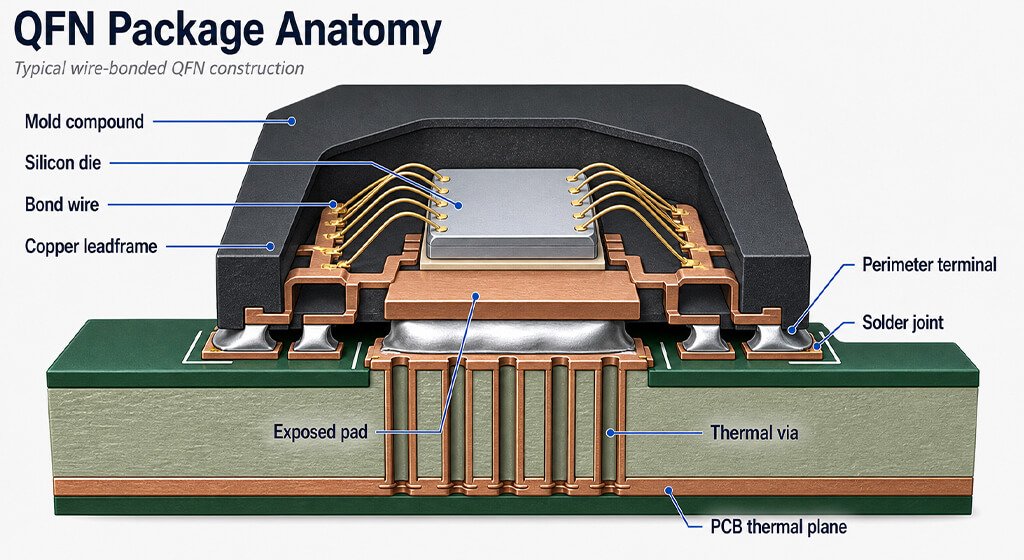
A typical leadframe-based QFN contains several elements:
- A silicon die that performs the device’s electrical function.
- A copper leadframe that supports the die and forms the external terminals.
- Wire bonds or another interconnect structure between the die and terminals.
- Mold compound that protects the internal structure.
- Perimeter terminals that connect the IC to PCB lands.
- An optional or standard exposed pad, depending on the package and device.
That description is typical, not universal. Analog Devices documents wire-bonded, flip-chip, and side-wettable QFN constructions in its QFN design and assembly guidance. Engineers should not assume every QFN has the same internal construction or terminal geometry.
2. Why Does a QFN Package Matter?
QFN packages is imporant because they combine a compact footprint, low profile, short electrical paths, and an efficient route for moving heat into the PCB.
Those advantages make QFNs useful in space-constrained, power-management, RF, sensing, and embedded applications.
Removing protruding leads reduces the area occupied by the package. It also shortens the path between the die, package terminals, and PCB.
Shorter interconnections can reduce parasitic inductance compared with longer formed leads, although designers must verify performance in the device data.
Many QFNs use an exposed metal pad beneath the package. When soldered to a matching PCB land, this pad can conduct heat into top-layer copper, thermal vias, and internal or backside planes. It may also provide a low-impedance electrical connection.
Do not assume the exposed pad is ground. Analog Devices notes that some exposed pads must connect to ground, some must remain electrically unconnected, and others permit more than one treatment. The exact exposed-pad instruction in the device datasheet takes priority.
QFN geometry also creates trade-offs. The low standoff leaves little room for flux volatiles to escape. Important solder joints are hidden after placement. Rework is harder than it is for a package with visible gull-wing leads. These are manageable manufacturing conditions, but they must be considered before layout release.
3. What Types of QFN Packages Are Available?
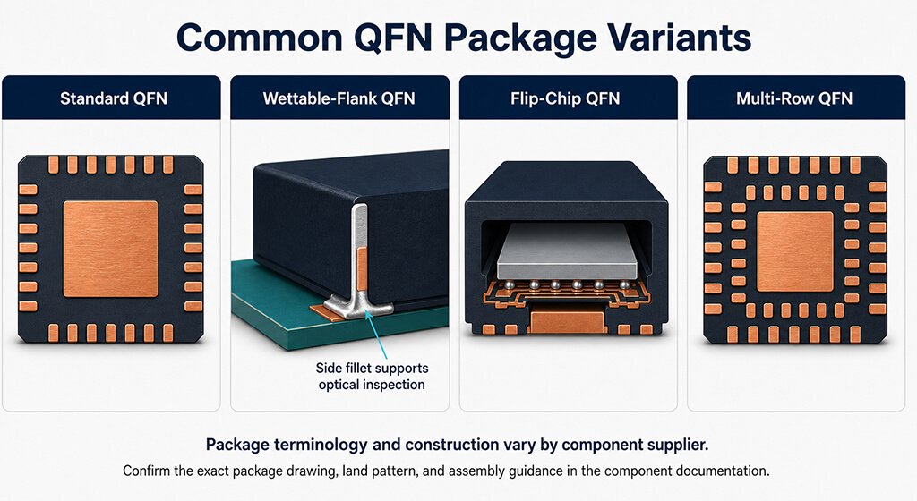
QFN is a package family rather than one fixed outline. Variants differ in body size, height, terminal count, pitch, terminal exposure, internal interconnection, and number of terminal rows.
Names such as VQFN or TQFN are not enough to build a footprint; the PCBA manufacturer’s package code, drawing, and recommended land pattern identify the actual geometry.
Common variations include:
- Single-row QFN: One row of terminals runs around the underside perimeter.
- Multi-row QFN: Two or more terminal rows increase I/O density without adopting a solder-ball array.
- Wire-bonded QFN: Bond wires connect the die to the leadframe terminals.
- Flip-chip QFN: The die uses a different internal interconnection approach, which can change the terminal pattern and thermal behavior.
- Sawn QFN: Packages are separated by sawing a molded array, often leaving exposed copper at the terminal edge.
- Punched QFN: Individual packages are formed through a punching or singulation process.
- Pull-back terminal QFN: The terminal ends stop short of the package edge, limiting visible solder fillets.
- Side-wettable-flank QFN: A plated or formed terminal feature promotes a visible side fillet after reflow.
Wettable flanks can improve automated optical inspection because a camera can evaluate the side fillet. They do not reveal the entire underside connection or the center pad. X-ray or other process controls may still be appropriate.
DFN and SON packages belong to the same broader leadless family, but their terminals usually occupy two opposing sides. QFN terminals occupy four sides. Device manufacturers may use different naming conventions, so the package drawing remains authoritative.
4. Which QFN PCB Design Parameters Matter Most?
The most important QFN design parameters are the exact terminal geometry, land pattern, exposed-pad connection, solder-mask design, thermal-via strategy, stencil apertures, paste volume, and inspection plan.
These choices interact. A change intended to improve heat transfer can increase solder loss, voiding, component float, or inspection difficulty if the full assembly process is not considered.
4.1. Start With the Exact Component Documentation
Confirm the manufacturer part number before creating or approving the footprint. Then review the package outline, recommended land pattern, pin-one convention, exposed-pad instruction, moisture-sensitivity information, and peak reflow classification.
Do not create a production footprint from a generic library name such as “QFN-32.” Two 32-terminal QFNs may use different body sizes, pitches, terminal lengths, pull-back dimensions, and exposed pads. Multi-source components require a land pattern that has been checked against every approved package.
IPC-7352 provides current generic land-pattern guidance, while IPC-7093A addresses BTC-specific implementation. A device manufacturer’s recommended land pattern may include package-specific requirements that a generic standard cannot predict.
4.2. Confirm the Exposed-Pad Function
The center land should match the relevant package drawing and electrical instruction. It is often part of the thermal path, but it can also carry ground or another specified potential.
Published package thermal data also depends on test conditions. For example, Texas Instruments explains that some QFN/SON thermal results use a defined multilayer test board. A thermal-resistance value is not independent of copper area, layers, vias, airflow, or measurement method.
4.3. Design Thermal Vias as Part of the System
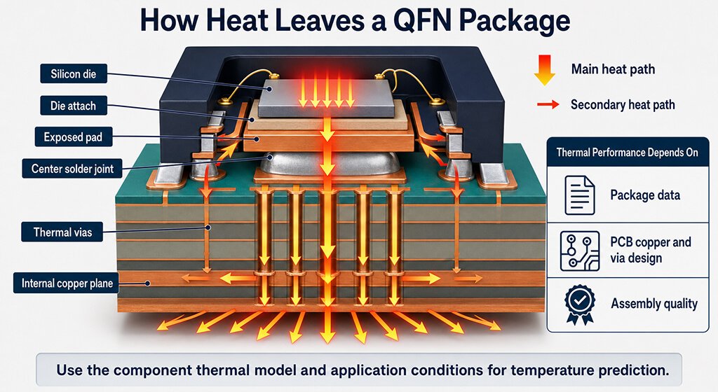
Thermal vias can move heat from the exposed pad into internal or backside copper. They can also draw molten solder away from the interface if their construction is not controlled.
Open vias, tented vias, plugged vias, filled vias, and capped via-in-pad structures behave differently during fabrication and reflow.
TI’s QFN and SON PCB Attachment guide treats its via patterns as starting points, not universal requirements. It states that the need for vias depends on device power dissipation.
The guide also recommends discussing plugging or tenting options with the PCB fabricator because those choices affect solder loss, trapped gas, cost, and process repeatability.
4.4. Coordinate the Land Pattern and Stencil
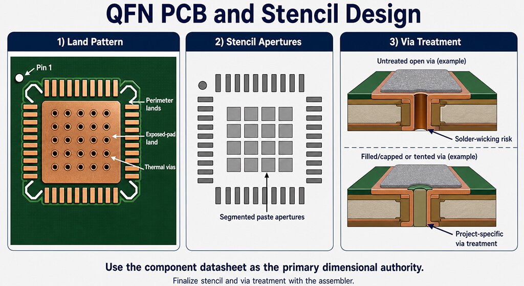
The copper land pattern defines where solder joints form. The stencil controls the solder volume delivered to those lands. A technically correct footprint can still produce defects if the apertures, foil thickness, paste type, and printing process do not work together.
IPC-7525C covers stencil thickness, aperture design, area ratio, step stencils, and fabrication methods. Small perimeter apertures need adequate paste release. The large center area usually needs controlled, segmented deposits rather than an unverified one-to-one opening.
Too much center-pad solder can raise or float the package. The perimeter terminals may then form opens. Too little paste can reduce thermal and mechanical contact. The correct balance depends on the component, stencil, solder paste, via construction, board finish, and validated printing process.
Design Decision | Why It Matters | Primary Authority | Project-Specific Confirmation |
Package Land Pattern | Controls alignment, solder-joint geometry, and spacing | Exact datasheet; IPC-7352 | Approved MPNs and assembler capability |
Exposed-Pad Connection | Affects function, grounding, and heat flow | Exact datasheet | Schematic and layout review |
Thermal-Via Construction | Affects heat transfer and solder loss | Device application note; IPC-7093A | PCB fabricator and thermal analysis |
Solder-Mask Definition | Affects copper tolerance and wettable area | Datasheet; package guidance | Board fabrication capability |
Stencil Foil And Apertures | Control paste release and volume | IPC-7525C; paste supplier | Printer, paste, and process trials |
Reflow Profile | Controls flux activation, wetting, and thermal exposure | IPC-7530B; paste and component data | Measured profile on a representative assembly |
Inspection Plan | Determines which hidden defects can be detected | IPC-7093A; customer requirements | Product class, risk, and sampling plan |
5. How Does QFN Compare With QFP, DFN, and BGA?
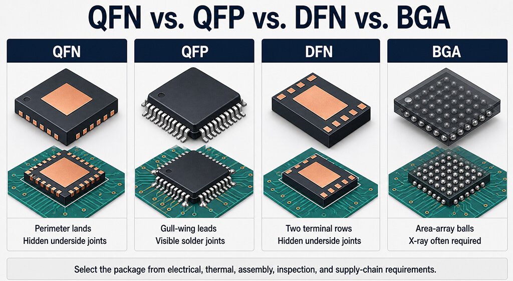
QFN usually offers a smaller outline and shorter interconnections than a comparable QFP, while QFP leads are easier to inspect and rework. DFN uses a similar bottom-terminated concept on two sides, and BGA supports much higher I/O density through a ball array.
The best choice depends on the available device, I/O count, thermal design, routing, prototype needs, and manufacturing capability.
Decision Factor | QFN | QFP | DFN/SON | BGA |
External Connection | Flat terminals around four underside edges | Gull-wing leads on four sides | Flat terminals on two underside edges | Solder balls under the body |
Board-Area Efficiency | High | Lower because leads project outward | Very high at lower I/O counts | High for dense I/O |
Typical I/O Range | Low to medium; multi-row options exist | Medium to high | Low to medium | Medium to very high |
Thermal Path | Often uses an exposed pad | Device-dependent | Often uses an exposed pad | Device and board dependent |
Optical Access | Limited; better with wettable flanks | Good for visible leads | Limited | Very limited |
Prototype Accessibility | More difficult | Usually easier | More difficult | More difficult |
Rework Complexity | Moderate to high | Lower | Moderate to high | High |
Common Reason To Choose It | Compact size, thermal path, short connections | Visibility and easier rework | Very compact two-sided terminal layout | High I/O density and routing efficiency |
QFN is not automatically better than QFP. A QFP may be the practical choice for early prototypes, educational boards, or products that prioritize direct probing and manual rework.
QFN becomes attractive when space, package height, heat transfer, or shorter electrical paths justify tighter assembly controls.
QFN and BGA comparisons also require caution. Package-level claims cannot establish which device has lower thermal resistance or better high-frequency performance.
Compare the actual parts, data-sheet conditions, board layouts, and required I/O count.
6. How Is a QFN Package Assembled on a PCB?
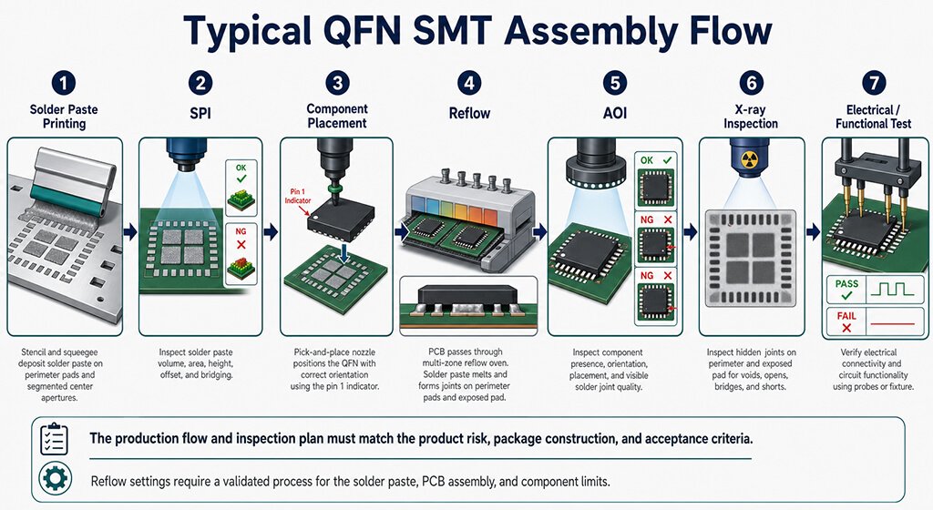
QFN assembly uses the standard SMT sequence: engineering review, solder-paste printing, paste inspection, automated placement, controlled reflow, post-reflow inspection, and electrical testing.
The equipment is familiar, but bottom terminals and the large center pad narrow the process window.
Stable results depend on measured paste deposits, an appropriate thermal profile, and inspection matched to hidden joints.
6.1. DFM and Production-Data Review
The engineer reviews the Gerber or intelligent PCB data, bill of materials, centroid file, assembly drawing, and inspection requirements.
QFN review should confirm pin one, package revision, footprint geometry, exposed-pad net, via treatment, stencil strategy, and test access.
6.2. Solder-Paste Printing and SPI
A stencil printer deposits solder paste on the perimeter lands and exposed-pad area.
Three-dimensional solder paste inspection, when used, measures deposit height, area, volume, and alignment before component placement.
SPI can identify blocked apertures, insufficient deposits, excessive paste, offsets, and suspected bridges. It cannot show the final solder joint because reflow has not occurred.
6.3. Automated Placement
The placement system identifies the component, checks orientation, and aligns it with the PCB.
QFN terminals provide limited visual access after placement, making correct package data and pin-one information especially important.
Surface tension can correct a small placement offset during reflow. It cannot compensate for the wrong footprint, a rotated part, severe paste imbalance, or incompatible terminal geometry.
6.4. Controlled Reflow
The assembly passes through a reflow oven, where flux activates and solder becomes liquid.
The profile must remain inside the solder-paste process window and the component’s thermal limits.
IPC-7530B covers temperature profiling for reflow and other mass-soldering processes. Zone setpoints alone do not prove that a QFN experienced the correct time-temperature history.
A representative assembly should be profiled because copper planes, board thickness, component mix, and loading affect actual temperatures.
6.5. Inspection and Testing
Post-reflow AOI can check component presence, orientation, alignment, visible edges, and wettable-flank fillets.
X-ray can examine hidden perimeter connections and center-pad solder distribution. Electrical tests then determine whether relevant nets or functions operate as intended.
Our AOI inspection guide explains what optical inspection can and cannot see. No single inspection method detects every QFN defect.
7. What QFN Defects Are Most Common, and How Are They Prevented?
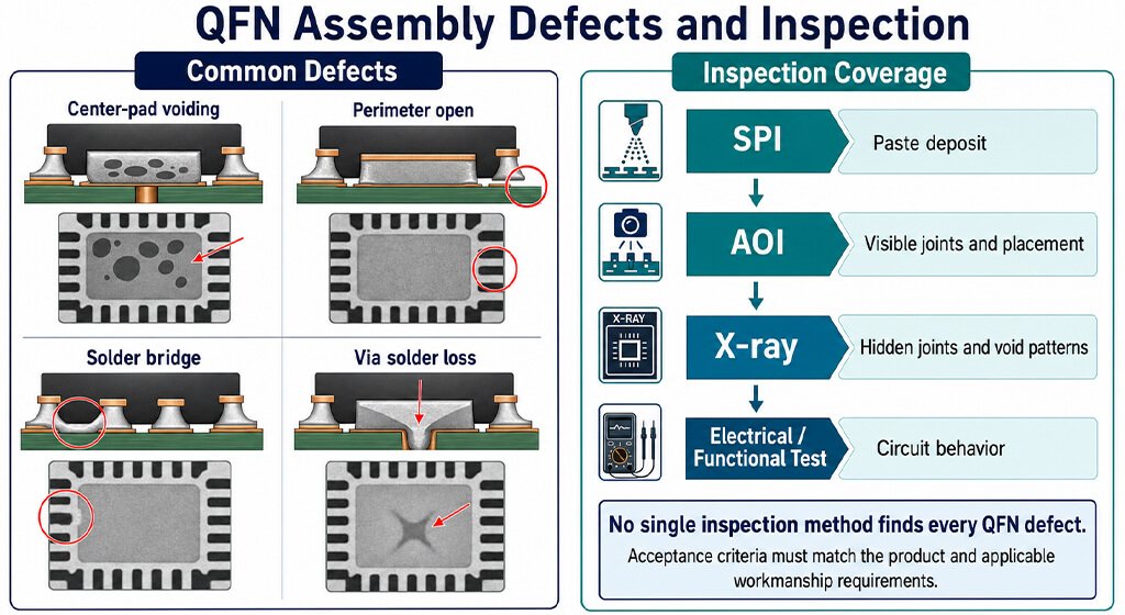
Common QFN defects include voiding, perimeter opens, bridging, solder starvation, package float, tilt, and incomplete wetting.
They rarely have one cause. Effective prevention links the component drawing, PCB footprint, via construction, stencil, paste chemistry, placement, thermal profile, and inspection results instead of treating each process step in isolation.
Defect | Common Contributors | Useful Detection Methods | Prevention Or Corrective Direction |
Center-Pad Voiding | Flux volatiles, pad geometry, paste chemistry, aperture pattern, profile | X-ray; thermal or functional evaluation when relevant | Segment apertures, review venting paths, test paste/profile combinations |
Perimeter Open | Package float, insufficient paste, contamination, poor wetting, wrong land pattern | X-ray, electrical test, functional test | Balance center and edge paste, verify footprint, improve printing and wetting |
Solder Bridge | Excess paste, aperture error, placement offset, low standoff | X-ray, AOI when edge-visible, electrical test | Correct apertures, stabilize printing, verify placement and pad spacing |
Solder Starvation | Paste wicking into vias, poor paste transfer, blocked apertures | SPI, X-ray, cross-section during failure analysis | Review via treatment, aperture release, foil thickness, and paste volume |
Package Float Or Tilt | Excess or unbalanced center-pad solder, unequal wetting | AOI, X-ray, height measurement | Balance deposits and validate stencil/reflow interaction |
Non-Wetting | Oxidation, contamination, expired materials, unsuitable thermal exposure | X-ray, visual edge evidence, failure analysis | Control storage, surface condition, flux activity, and profile |
Inspection Escape | Hidden joints, unsuitable angle or method, unclear criteria | Audit across SPI, AOI, X-ray, ICT/FCT | Define the inspection strategy before production |
Voiding deserves careful wording. Some voiding can occur because flux gases become trapped as the joint forms. Its effect depends on location, size, distribution, current density, heat flow, mechanical loading, and product requirements.
There is no responsible universal void limit for every QFN and application. IPC-7093A includes guidance for voids in BTC thermal or ground planes, while device manufacturers may publish their own recommendations. Contractual acceptance criteria should be agreed before production when voiding is critical.
Solder-paste suppliers also show why one number cannot predict results. Indium Corporation reports that QFN voiding varies with profile, flux chemistry, alloy, PCB surface finish, design, and the component itself. Material test data should be treated as evidence for that tested system, not a guaranteed result on another production line.
8. Where Are QFN Packages Commonly Used?
QFN packages are common in power management, RF transceivers, wireless modules, sensors, motor control, automotive electronics, portable medical devices, and embedded systems.
They fit products that value compact dimensions, low package height, short interconnections, or an efficient PCB thermal path. Suitability still depends on environment, serviceability, sourcing, and the assembler’s process capability.
9. What Should Engineers Check Before Releasing a QFN Design?
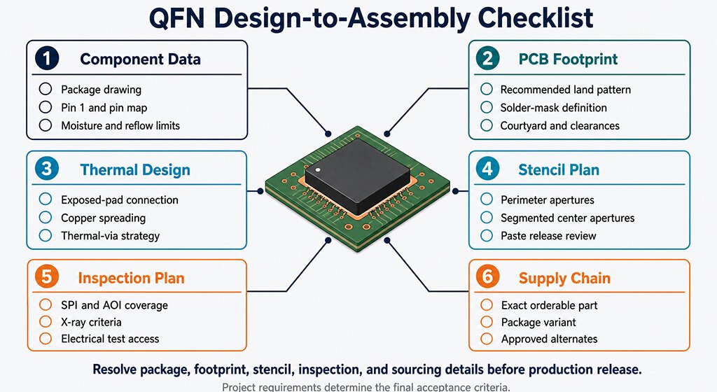
Before release, engineers should verify the exact package, footprint, exposed-pad net, thermal path, via construction, stencil assumptions, moisture controls, reflow limits, inspection coverage, and test plan.
The checklist should travel with the controlled manufacturing data.
Resolving these items before stencil fabrication costs less than diagnosing hidden opens or thermal failures after assembly.
QFN Design and DFM Checklist
- The exact manufacturer part number and package code are approved.
- Every approved alternate has been checked against the PCB footprint.
- The current manufacturer package drawing has been reviewed.
- Pin one is consistent across schematic, footprint, centroid file, and assembly drawing.
- The exposed-pad electrical connection follows the device datasheet.
- The thermal design reflects actual power, copper, airflow, and board construction.
- Thermal-via type, diameter, pitch, filling, capping, or tenting has been reviewed with the PCB fabricator.
- The land pattern and solder-mask design match component and manufacturing requirements.
- The stencil design balances perimeter and center-pad solder volumes.
- Aperture area ratio and paste-release capability have been checked.
- The surface finish supports the selected pitch and assembly process.
- -Moisture sensitivity, floor life, storage, and baking instructions are documented.
- A representative reflow profile will be measured, not inferred from oven settings.
- SPI, AOI, X-ray, electrical test, and functional test responsibilities are defined.
- Any voiding or hidden-joint acceptance criteria are stated in the purchase documentation.
- Rework restrictions and maximum permitted thermal exposures are understood.
10. How Can PCBSAIL Support a QFN Assembly Project?

PCBSAIL can support QFN projects through DFM review, solder-paste inspection, controlled SMT placement and reflow, AOI, X-ray inspection for hidden joints, and project-defined electrical or functional testing.
The appropriate process depends on the exact component, PCB design, production volume, and acceptance requirements, so capability review should occur before stencil release.
For quotation and DFM review, prepare the Gerber or intelligent PCB data, bill of materials, centroid file, assembly drawing, and any special QFN acceptance requirements.
If the exposed pad has a critical electrical or thermal role, include the schematic, device application note, and test expectations.
Welcome submit the design for review. Our review can identify footprint, stencil, via, inspection, and data issues before they become hidden assembly defects.
11. FAQ About PCB Pads
Does every QFN have an exposed thermal pad?
No. Many QFN devices include an exposed center pad, but package configurations vary. IPC-7093A includes BTC examples both with and without thermal pads. Always inspect the exact package drawing instead of creating a center land from a generic QFN footprint.
Should the QFN exposed pad connect to ground?
Only when the device documentation says so. Many exposed pads connect to ground, but others use a different potential or must remain unconnected. The schematic symbol, PCB net, land pattern, and thermal-via network must follow the exact component datasheet.
What is the difference between QFN and QFP?
QFN terminals sit beneath the package edges, while QFP gull-wing leads extend outside the body. QFN usually occupies less board area and can provide a strong thermal path. QFP leads are easier to inspect, probe, and rework, which may benefit prototypes and lower-complexity assembly.
Can a QFN package be hand-soldered?
A skilled technician may assemble some QFN prototypes with suitable paste, heating, and inspection. Reliable access to an electrically connected center pad remains difficult. For repeatable production, controlled solder-paste printing, placement, reflow, and appropriate inspection are safer than relying on a soldering iron.
Why do QFN solder joints develop voids?
Voids can form when flux volatiles remain trapped as the low-standoff center-pad joint solidifies. Aperture pattern, paste volume, flux chemistry, surface finish, via construction, wetting, and reflow profile can all contribute. The acceptable result depends on thermal, electrical, mechanical, and contractual requirements.
References
– IPC, IPC-7093A: Design and Assembly Process Implementation for Bottom Termination Components
– IPC, Document Revision Table, including IPC-7352, IPC-7525C, and IPC-7530B status.
– IPC, J-STD-001J and IPC-A-610J release notice
– Texas Instruments, QFN and SON PCB Attachment, Rev. C
– NXP Semiconductors, AN1902: Assembly Guidelines for QFN and SON Packages
– Microchip Technology, AN2089: Package Application Note for QFN and DFN Packages
– Analog Devices, [Exposed Pads: A Brief Introduction.
– JEDEC, Standards, publications, and registered package outlines
– Indium Corporation, technical resources on void reduction.